


世界中の半導体製造業者が頼る露光装置メーカー「ASML」はどんな会社なのか
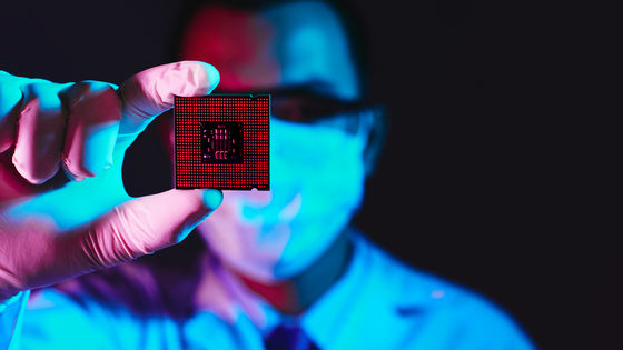
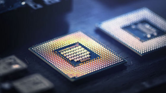
半導体を注文して納品されるまでにかかるリードタイムが20週間を超えるなど、半導体不足は悪化する一方です。最先端の半導体を製造するには1台が160億円以上する非常に高価な製造装置「EUV」が必要ですが、EUV装置の供給は「ASML」という時価総額30兆円以上のオランダの会社がほぼ独占しています。ASMLがどんな企業なのかについての解説を、Twitter上でTrungTPhanさんが行っています。
ASML is the most important company you've never heard of.
— Trung Phan ???????? (@TrungTPhan) 2021年8月22日
The $300B+ Dutch firm makes the machines that make semiconductors. Each one costs $150m and access to them are a huge geopolitical flashpoint.
Here's a breakdown ???? pic.twitter.com/pARj3x7Kwo
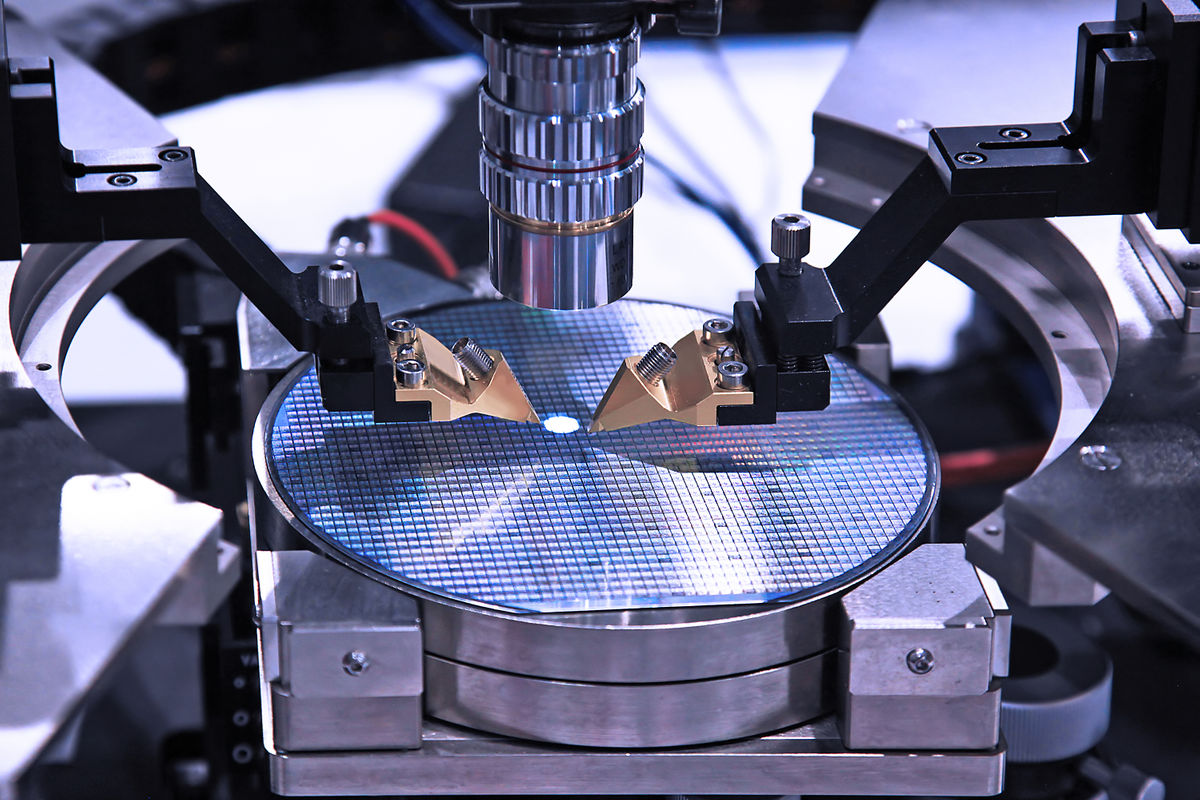
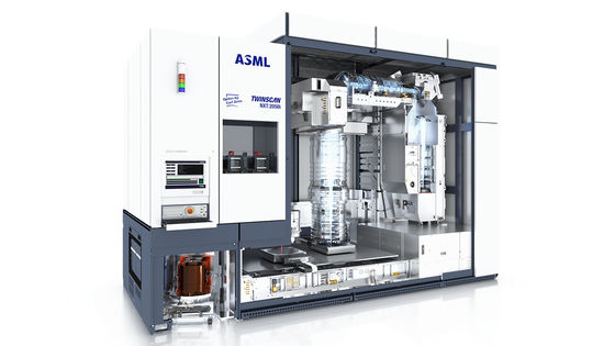
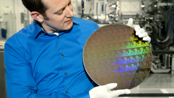
ASMLの主要製品は高度な光技術を使用して極小回路をシリコンウエハーに印刷する極端紫外線リソグラフィ(EUV)装置です。EUV装置の製造台数は年間50台ほどで、ASMLが技術をほぼ独占しています。
1/ What *exactly* does ASML sell?
— Trung Phan ???????? (@TrungTPhan) 2021年8月22日
Its key product is an extreme ultraviolet lithography (EUV) machine, which uses advanced light technology to "print" tiny circuits onto Silicon wafers.
Only ~50 are made a year and ASML has a near monopoly on the machine technology. pic.twitter.com/M6xL6QiDzX
ASMLの主なクライアントはIntelやSamsung、TSMCなどの半導体企業で、ムーアの法則に従ってコンピューティングを進化させ続けるためにEUVが必要です。ASMLは2020年に160億ドル(約1兆8000億円)を売り上げました。
2/ You def know ASML's main clients: Intel, Samsung and Taiwan Semiconductor Manufacturing Co. (TSMC).
— Trung Phan ???????? (@TrungTPhan) 2021年8月22日
They need EUV to keep Moore's Law ("# of transistors on microchips doubles every 2 years") alive and continue to advance computing.
Total ASML sales in 2020 = $16B+. pic.twitter.com/1tt9hXCFgL
ASMLは1984年にフィリップスとASMインターナショナルとの間の合弁会社として設立されました。フィリップスの建物の後ろにある小屋で立ち上げられるなど、非常に控えめなスタートだったとのこと。
3/ The ASML story begins in 1984, as a joint venture between Dutch conglomerate Philips and an electronics maker called Advanced Semiconductor Materials Int.
— Trung Phan ???????? (@TrungTPhan) 2021年8月22日
The project had a very humble start: it was launched in a shed behind a Philip's building in Eindhoven, Netherlands. pic.twitter.com/9uYMZooHVW
ASMLの最初の製品はシリコンに設計を投影するプロジェクター(半導体露光器)「PA 2000ステッパー」でした。しかし何年も、半導体露光器は日本の競合メーカーであるニコンやキヤノンに後れを取っていました。1990年にASMLは親会社との資本関係を解消し、独立企業になります。
4/ The venture's first product was called the PA 2000 stepper (think a slide projector "projecting" designs on silicon).
— Trung Phan ???????? (@TrungTPhan) 2021年8月22日
For years, the product failed to make headway against leading Japanese competitors (Nikon, Canon) and, in 1990, ASML was spun out as its own company. pic.twitter.com/hKsQTjS4f0
ASMLの最初のヒット製品は1991年に登場し、その勢いでASMLは1995年に上場を行います。上場後、いくつものアメリカのリソグラフィ企業を買収し、1990年代の終わりにはNikonやCanonに並ぶマーケットシェアを獲得していました。さらにASMLは一歩抜け出すための2つの大きな賭けをします。
5/ ASML scored its 1st hit product in 1991, giving it momentum to IPO in 1995.
— Trung Phan ???????? (@TrungTPhan) 2021年8月22日
Soon after, it acquired a # of US lithography firms and -- by the end of 1990s -- it had comparable market share to Nikon and Canon.
From there, ASML made 2 big bets that separated it from the pack. pic.twitter.com/fWbm2ria7P
最初の賭けとして、ASMLは2006年に液浸リソグラフィを利用したTWINSCANシステムを開発。液浸リソグラフィは水をレンズとして利用することでレーザーの波長を短縮し、よりチップ上の回路を増加させる技術です。TWINSCANはASMLの初めての先進的な製品だったとのこと。
6/ Both bets were made to keep up with Moore's law.
— Trung Phan ???????? (@TrungTPhan) 2021年8月22日
First: In 2006, ASML released its TWINSCAN system using immersion lithography (it utilizes water as lens to shrink the laser's wavelength = more circuits on chip).
It was ASML's first market-leading product. pic.twitter.com/Ny8VNeJwed
そして2000年代の半ばに、ASMLはEUV技術の開発に巨額の投資を行います。EUVリソグラフィを使うにはSamsungやIntel、TSMCが工場を完全に再設計・再構築する必要があるため、EUV技術への投資は大きなリスクでした。ASMLは2008年から2014年にかけて、50億ドル(約6000億円)をEUV技術の研究に投資しています。
7/ Also in the mid-2000s, ASML started spending huge R&D on EUV technology.
— Trung Phan ???????? (@TrungTPhan) 2021年8月22日
It was a massive risk, though: EUV lithography would require Samsung, Intel and TMSC to completely rebuild and redesign their fabrication plants.
From 2008-14, ASML put $5B+ into EUV research. pic.twitter.com/uegqrqAEfp
EUV技術に必要な科学が確立されたのは1980年代のことで、アメリカのエネルギー省とAMDやIBM、Intelといった企業によるアメリカ主導の取り組みでした。そしてASMLが1999年にライセンスを取得しています。Canonは資金面の問題でEUVを追求しないことを決定し、Nikonは古い技術をより洗練させることを選択しました。
8/ The science behind EUV was established in the late 1980s. It was a US-led effort between the Dept. of Energy and industry (e.g. AMD, IBM, Intel).
— Trung Phan ???????? (@TrungTPhan) 2021年8月22日
ASML licensed EUV tech in 1999. Canon elected not to pursue it due to financial problems while Nikon chose to develop older tech. pic.twitter.com/tdS2oMriPw
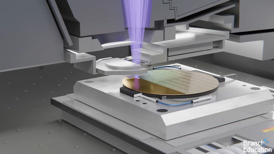
EUVの動作は下記の通り。
・スズの滴が真空に落ちる
・高出力レーザーのパルスを照射
・スズ原子がイオン化されてプラズマを形成
・鏡がプラズマから放出されるEUVをキャプチャ
・鏡が波長13.5nmのEUVをウエハーに転送
9/ How EUV works today:
— Trung Phan ???????? (@TrungTPhan) 2021年8月22日
◻️ A tin droplet drops into a vacuum
◻️ It's pulsed by a high-power laser
◻️ Tin atoms are ionized, creating plasma
◻️ A mirror captures EUV radiation emitted by plasma
◻️ Mirror transfers EUV to wafer (wavelength=13.5 nanometers, basically X-ray level) pic.twitter.com/sFC4d1fGZb
EUVの可能性は非常に大きかったため、IntelとSamsung、TSMCなどの企業は共同でASMLの株式の23%を取得しました。最も多くを取得したIntelは250億ユーロ(約3兆2000億円)で15%を取得。なお、この時取得された株式のほとんどは既に売却されています。最初の商用EUV製品は2016年にリリースされました。
10/ The potential of EUV was so great that Intel, Samsung and TMSC -- all competitors -- jointly acquired 23% of ASML.
— Trung Phan ???????? (@TrungTPhan) 2021年8月22日
Intel put up the most: €2.5B for a 15% share (today, the firms have sold down most their stakes).
The first production-ready EUV machine was released in 2016. pic.twitter.com/k1ldaNxuE6
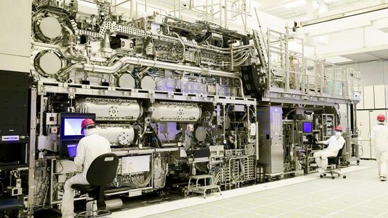
ASMLは、同じ「100億円以上の商品」を扱う航空業界のボーイングと似た役割を果たしており、アメリカの工作機械や日本の化学薬品、ドイツのレンズなど4750のグローバルな高価値部品サプライヤーのインテグレーターとなっています。なお、NikonやCannonはほとんどの生産を社内で行っているとのこと。
11/ Why are EUVs so expensive?
— Trung Phan ???????? (@TrungTPhan) 2021年8月22日
ASML plays a role similar to Boeing for airplanes (also $100m+ products): it's an integrator of 4750 global high-value parts suppliers:
◻️ Tooling equipment (US)
◻️ Chemicals (Japan)
◻️ Lens (Germany)
(Nikon/Cannon do most production in-house) pic.twitter.com/SSOsZ7RzgS
また、ASMLがEUVを年間50台しか生産できないのには下記の理由があるそうです。
・何千ものサプライヤーを調整するのが非常に困難
・それぞれの装置がカスタム可能で、30以上の変数を選択可能
・ツァイスレンズのような特殊部品の生産に40週間かかるなどリードタイムが長い
12/ Why can ASML only produce 50 EUV machines a year?
— Trung Phan ???????? (@TrungTPhan) 2021年8月22日
◻️ Co-ordinating 1000s of suppliers is very difficult (just like an aircraft)
◻️ Each machine is custom (30+ variables to choose from)
◻️ Lead-time are long (speciality parts like the Zeiss lens takes 40 weeks to produce) pic.twitter.com/jKubNGXj1p
さらに納品も下記のように大変とのこと。
・それぞれのEUVの重量は180トン
・分解されたEUVは40個のコンテナを利用
・輸送には20個のトラックと3台のボーイング747が必要
・ASMLチームが管理のために現場にいる必要がある
・EUVを収容するには最低10億ドル(約1100億円)必要
13/ The delivery process is nuts, too:
— Trung Phan ???????? (@TrungTPhan) 2021年8月22日
◻️ Each EUV weighs 180 tons
◻️ A disassembled EUV takes up 40 shipping containers
◻️ Shipping it (mostly to Asia) takes 20 trucks and 3 Boeing 747s
◻️ ASML teams must be on-the-ground to maintain them
◻️ The min spend to house EUVs is $1B pic.twitter.com/pXALTy5sbY
2021年時点ではASMLはEUVおよびDeep UVの半導体リソグラフィ分野で90%シェアを獲得しています。半導体分野では毎年1200億ドル(約13兆円)以上の設備投資が見込まれており、今後も自動車など主要セクターの成長や、よりEUVを必要とする5nmプロセスへの移行などEUVへの追い風は巨大です。
14/ Today, ASML has a 90% share in semi lithography (EUV and Deep UV).
— Trung Phan ???????? (@TrungTPhan) 2021年8月22日
EUV tailwinds are huge:
◻️ Semi CAPEX >$120B+ in 2021 (similar spend in following years)
◻️ Key sectors (esp. auto AKA Tesla chips) will see growth for years
◻️ Transition to 5nm process requires more EUV pic.twitter.com/9pFgKGP0Us
EUV装置自体の販売がゆっくりだとしても、ASMLの事業はシステムのメンテナンスや移行、アップグレードにシフトしているとのこと。ASMLの機械の20年の寿命の中で、サービスベースの売り上げは装置価格の50%に到達する可能性もあるようです。
15/ Even if machine sales slow, ASML's business is increasingly shifting to system maintenance, relocation and upgrades.
— Trung Phan ???????? (@TrungTPhan) 2021年8月22日
Over a 20yr lifespan of an ASML machine, services-based sales may reach 50% of the initial machine price (w/ high margins)...across a growing installed base. pic.twitter.com/glPMmhTsah
チップはデータセンターやAI、自動車、マイニングなど全ての分野に必要なため、半導体は21世紀の石油です。EUVライセンス技術をオランダから中国へ輸出することはアメリカに禁止されるほどで、技術冷戦が過熱するにつれ、小屋から出発して30兆円規模の企業に成長したASMLの名前を聞く機会がこれまで以上に増えそうです。
16/ With chips needed in everything (data centres, AI, autos, mining), semis are the OIL of the 21st century.
— Trung Phan ???????? (@TrungTPhan) 2021年8月22日
The US has even blocked Dutch exports of EUV-licensed tech to China. As the Tech Cold War heats up, expect to hear more of ASML: the $300B+ giant that started in a shed. pic.twitter.com/YbwiPNErtB
TrungTPhanさんはスレッドの続きでデータの出典やディスカッションポッドキャストなどの情報をツイートしているので、気になる人は確認してみてください。
・関連記事
アメリカVS中国の半導体開発競争で鍵を握るオランダ企業の精密機械とは? - GIGAZINE
中国の半導体メーカーが約2兆円超の負債を抱えたまま操業前に破綻、巨額詐欺の実態とは? - GIGAZINE
新型コロナウイルス感染症は半導体産業にどのような影響を与えたのか? - GIGAZINE
Intelのファウンドリサービス拡充戦略「IDM2.0」はIntel復活の糸口となるのか? - GIGAZINE
PlayStation 5や自動車の生産に影響を与える世界的な半導体不足の理由とは? - GIGAZINE
「ムーアの法則」の限界を回避できる期待の製造技術「EUVリソグラフィ」とは? - GIGAZINE
・関連コンテンツ
in ハードウェア, Posted by log1d_ts
You can read the machine translated English article What kind of company is the exposure equ….