What kind of company is the exposure equipment manufacturer 'ASML' that semiconductor manufacturers around the world rely on?
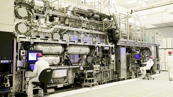
The semiconductor shortage is only getting worse, as the lead time for ordering and delivering semiconductors exceeds 20 weeks. To manufacture cutting-edge semiconductors, one unit requires a very expensive manufacturing equipment 'EUV ' that costs more than 16 billion yen, but EUV equipment is supplied by a Dutch company called 'ASML ' that has a market capitalization of more than 30 trillion yen. Is almost monopolized. TrungTPhan explains on Twitter what kind of company ASML is.
ASML is the most important company you've never heard of.
— Trung Phan ?????????? (@TrungTPhan) August 22, 2021
The $ 300B + Dutch firm makes the machines that make semiconductors. Each one costs $ 150m and access to them are a huge geopolitical flashpoint.
Here's a breakdown ???? pic.twitter.com/pARj3x7Kwo
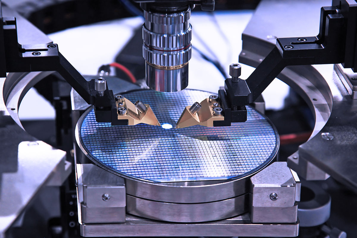
ASML's flagship product is extreme ultraviolet lithography (EUV) equipment that uses advanced optical technology to print tiny circuits on silicon wafers. EUV equipment is manufactured about 50 units a year, and ASML almost monopolizes the technology.
1 / What * exactly * does ASML sell?
— Trung Phan ?????????? (@TrungTPhan) August 22, 2021
Its key product is an extreme ultraviolet lithography (EUV) machine, which uses advanced light technology to 'print' tiny circuits onto Silicon wafers.
Only ~ 50 are made a year and ASML has a near monopoly on the machine technology. Pic.twitter.com/M6xL6QiDzX
ASML's main clients are semiconductor companies such as Intel, Samsung and TSMC, which require EUV to keep computing evolving according to Moore's Law. ASML sold $ 16 billion in 2020.
2 / You def know ASML's main clients: Intel, Samsung and Taiwan Semiconductor Manufacturing Co. (TSMC).
— Trung Phan ?????????? (@TrungTPhan) August 22, 2021
They need EUV to keep Moore's Law ('# of transistors on microchips doubles every 2 years') alive and continue to advance computing.
Total ASML sales in 2020 = $ 16B +. Pic.twitter.com/1tt9hXCFgL
ASML was founded in 1984 as a joint venture between Philips and ASM International. It was a very modest start, such as being launched in a hut behind the Philips building.
3 / The ASML story begins in 1984, as a joint venture between Dutch conglomerate Philips and an electronics maker called Advanced Semiconductor Materials Int.
— Trung Phan ?????????? (@TrungTPhan) August 22, 2021
The project had a very humble start: it was launched in a shed behind a Philip's building in Eindhoven, Netherlands. Pic.twitter.com/9uYMZooHVW
ASML's first product was the PA 2000 Stepper, a projector (semiconductor exposure device) that projects designs onto silicon. But for years, semiconductor exposures have fallen behind Japanese competitors Nikon and Canon. In 1990 ASML dissolved its capital relationship with its parent company and became an independent company.
4 / The venture's first product was called the PA 2000 stepper (think a slide projector 'projecting' designs on silicon).
— Trung Phan ?????????? (@TrungTPhan) August 22, 2021
For years, the product failed to make headway against leading Japanese competitors (Nikon, Canon) and, in 1990, ASML was spun out as its own company. Pic.twitter.com/hKsQTjS4f0
ASML's first hit product appeared in 1991, and ASML went public in 1995 with that momentum. After listing, it acquired a number of American lithography companies, gaining market share alongside Nikon and Canon in the late 1990s. In addition, ASML makes two big bets to get out of the way.
5 / ASML scored its 1st hit product in 1991, giving it momentum to IPO in 1995.
— Trung Phan ?????????? (@TrungTPhan) August 22, 2021
Soon after, it acquired a # of US lithographic firms and --by the end of 1990s --it had comparable market share to Nikon and Canon.
From there, ASML made 2 big bets that separated it from the pack. Pic.twitter.com/fWbm2ria7P
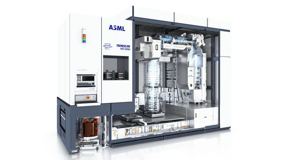
As a first bet, ASML developed the TWINSCAN system in 2006 using immersion lithography. Immersion lithography is a technology that uses water as a lens to shorten the wavelength of the laser and increase the number of circuits on the chip. TWINSCAN was ASML's first advanced product.
6 / Both bets were made to keep up with Moore's law.
— Trung Phan ?????????? (@TrungTPhan) August 22, 2021
First: In 2006, ASML released its TWINSCAN system using immersion lithography (it utilizes water as lens to shrink the laser's wavelength = more circuits on chip).
It was ASML's first market-leading product. Pic.twitter.com/Ny8VNeJwed
And in the mid-2000s, ASML made a huge investment in the development of EUV technology. Investing in EUV technology was a big risk as Samsung, Intel and TSMC had to completely redesign and rebuild their factories to use EUV lithography. ASML has invested $ 5 billion in EUV technology research between 2008 and 2014.
7 / Also in the mid-2000s, ASML started spending huge R & D on EUV technology.
— Trung Phan ?????????? (@TrungTPhan) August 22, 2021
It was a massive risk, though: EUV lithography would require Samsung, Intel and TMSC to completely rebuild and redesign their fabrication plants.
From 2008-14, ASML put $ 5B + into EUV research. Pic.twitter.com/uegqrqAEfp
The science required for EUV technology was established in the 1980s, a US-led initiative by the US Department of Energy and companies such as AMD, IBM, and Intel. And ASML was licensed in 1999. Canon decided not to pursue EUV due to financial issues, and Nikon chose to refine the old technology.
8 / The science behind EUV was established in the late 1980s. It was a US-led effort between the Dept. of Energy and industry (eg AMD, IBM, Intel).
— Trung Phan ?????????? (@TrungTPhan) August 22, 2021
ASML licensed EUV tech in 1999. Canon elected not to pursue it due to financial problems while Nikon chose to develop older tech. Pic.twitter.com/tdS2oMriPw
The operation of EUV is as follows.
・ Tin drops fall into a vacuum
・ Irradiate high-power laser pulse
・ Tin atoms are ionized to form plasma
・ Mirror captures EUV emitted from plasma
・ The mirror transfers EUV with a wavelength of 13.5 nm to the wafer.
9 / How EUV works today:
— Trung Phan ?????????? (@TrungTPhan) August 22, 2021
◻️ A tin droplet drops into a vacuum
◻️ It's pulsed by a high-power laser
◻️ Tin atoms are ionized, creating plasma
◻️ A mirror captures EUV radiation emitted by plasma
◻️ Mirror transfers EUV to wafer (wavelength = 13.5 nanometers, basically X-ray level) pic.twitter.com/sFC4d1fGZb
EUV was so promising that companies such as Intel, Samsung and TSMC jointly acquired a 23% stake in ASML. Intel, which acquired the most, acquired 15% for 25 billion euros (about 3.2 trillion yen). Most of the shares acquired at this time have already been sold. The first commercial EUV product was released in 2016.
10 / The potential of EUV was so great that Intel, Samsung and TMSC --all competitors --jointly acquired 23% of ASML.
— Trung Phan ?????????? (@TrungTPhan) August 22, 2021
Intel put up the most: € 2.5B for a 15% share (today, the firms have sold down most their stakes).
The first production-ready EUV machine was released in 2016. pic.twitter.com/k1ldaNxuE6
ASML plays a role similar to Boeing in the aviation industry, which handles the same 'goods over 10 billion yen', and is an integrator of 4750 global high-value parts suppliers such as American machine tools, Japanese chemicals, and German lenses. It has become. In addition, Nikon and Canon are said to be doing most of the production in-house.
11 / Why are EUVs so expensive?
— Trung Phan ?????????? (@TrungTPhan) August 22, 2021
ASML plays a role similar to Boeing for airplanes (also $ 100m + products): it's an integrator of 4750 global high-value parts suppliers:
◻️ Tooling equipment (US)
◻️ Chemicals (Japan)
◻️ Lens (Germany)
(Nikon / Canon do most production in-house) pic.twitter.com/SSOsZ7RzgS
In addition, ASML can produce only 50 EUVs a year for the following reasons.
· Very difficult to coordinate thousands of suppliers
・ Each device can be customized, and more than 30 variables can be selected.
・ Long lead time, such as 40 weeks to produce special parts such as Zeiss lenses
12 / Why can ASML only produce 50 EUV machines a year?
— Trung Phan ?????????? (@TrungTPhan) August 22, 2021
◻️ Co-ordinating 1000s of suppliers is very difficult (just like an aircraft)
◻️ Each machine is custom (30+ variables to choose from)
◻️ Lead-time are long (speciality parts like the Zeiss lens takes 40 weeks to produce) pic.twitter.com/jKubNGXj1p
Furthermore, delivery is also difficult as shown below.
・ Each EUV weighs 180 tons
・ Disassembled EUV uses 40 containers
・ 20 trucks and 3 Boeing 747s are required for transportation
· ASML team needs to be on site for management
・ At least 1 billion dollars (about 110 billion yen) is required to accommodate EUV
13 / The delivery process is nuts, too:
— Trung Phan ?????????? (@TrungTPhan) August 22, 2021
◻️ Each EUV weighs 180 tons
◻️ A disassembled EUV takes up 40 shipping containers
◻️ Shipping it (mostly to Asia) takes 20 trucks and 3 Boeing 747s
◻️ ASML teams must be on-the-ground to maintain them
◻️ The min spend to house EUVs is $ 1B pic.twitter.com/pXALTy5sbY
As of 2021, ASML has a 90% share of EUV and Deep UV semiconductor lithography. In the semiconductor field, capital investment of more than 120 billion dollars (about 13 trillion yen) is expected every year, and the tailwind for EUV such as the growth of major sectors such as automobiles and the shift to the 5nm process that requires more EUV will continue. It's huge.
14 / Today, ASML has a 90% share in semilithography (EUV and Deep UV).
— Trung Phan ?????????? (@TrungTPhan) August 22, 2021
EUV tailwinds are huge:
◻️ Semi CAPEX> $ 120B + in 2021 (similar spend in following years)
◻️ Key sectors (esp. Auto AKA Tesla chips) will see growth for years
◻️ Transition to 5nm process requires more EUV pic.twitter.com/9pFgKGP0Us
Even if the EUV equipment itself is sold slowly, ASML's business is shifting to system maintenance, migration and upgrades. During the 20-year life of ASML machines, service-based sales could reach 50% of the equipment price.
15 / Even if machine sales slow, ASML's business is gradually shifting to system maintenance, relocation and upgrades.
— Trung Phan ?????????? (@TrungTPhan) August 22, 2021
Over a 20yr lifespan of an ASML machine, services-based sales may reach 50% of the initial machine price (w / high margins) ... across a growing installed base. Pic.twitter.com/glPMmhTsah
Semiconductors are oil for the 21st century, as chips are needed in all areas such as data centers, AI, automobiles, and mining. Exporting EUV licensed technology from the Netherlands to China has been banned by the United States, and as the Cold War overheated, we have had the opportunity to hear the name of ASML, which started from a hut and grew into a 30 trillion yen company. It seems to increase more than that.
16 / With chips needed in everything (data centers, AI, autos, mining), semis are the OIL of the 21st century.
— Trung Phan ?????????? (@TrungTPhan) August 22, 2021
The US has even blocked Dutch exports of EUV-licensed tech to China. As the Tech Cold War heats up, expect to hear more of ASML: the $ 300B + giant that started in a shed. Pic.twitter.com/YbwiPNErtB
TrungTPhan tweeted information such as data sources and discussion podcasts in the continuation of the thread, so please check it if you are interested.
Related Posts:
in Hardware, Posted by log1d_ts