A movie that follows the back side of the most amazing machine 'EUV system' in Intel history is on sale
Intel has released a movie that approaches the 'EUV system', which is said to be 'the most precise and complicated machine in Intel'. EUV is a technology for pursuing
EUV: The Most Precise, Complex Machine at Intel
https://www.intel.com/content/www/us/en/newsroom/news/euv-most-precise-complex-machine.html
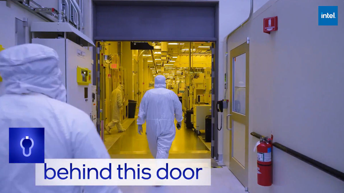
Behind this Door: Learn about EUV, Intel's Most Precise, Complex Machine --YouTube
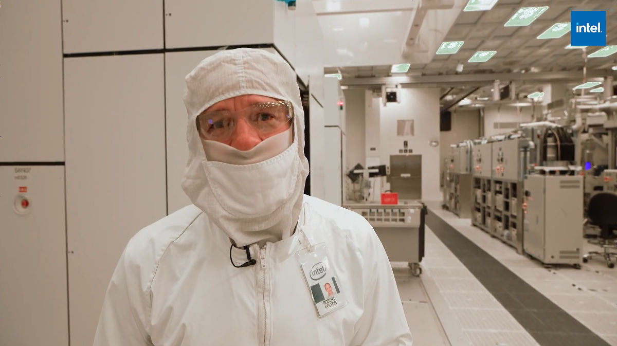
Rob Kelton has been reporting on Intel's products and the amazing machines that make them for 21 years. Even with Mr. Kelton, the EUV system is 'amazing'.
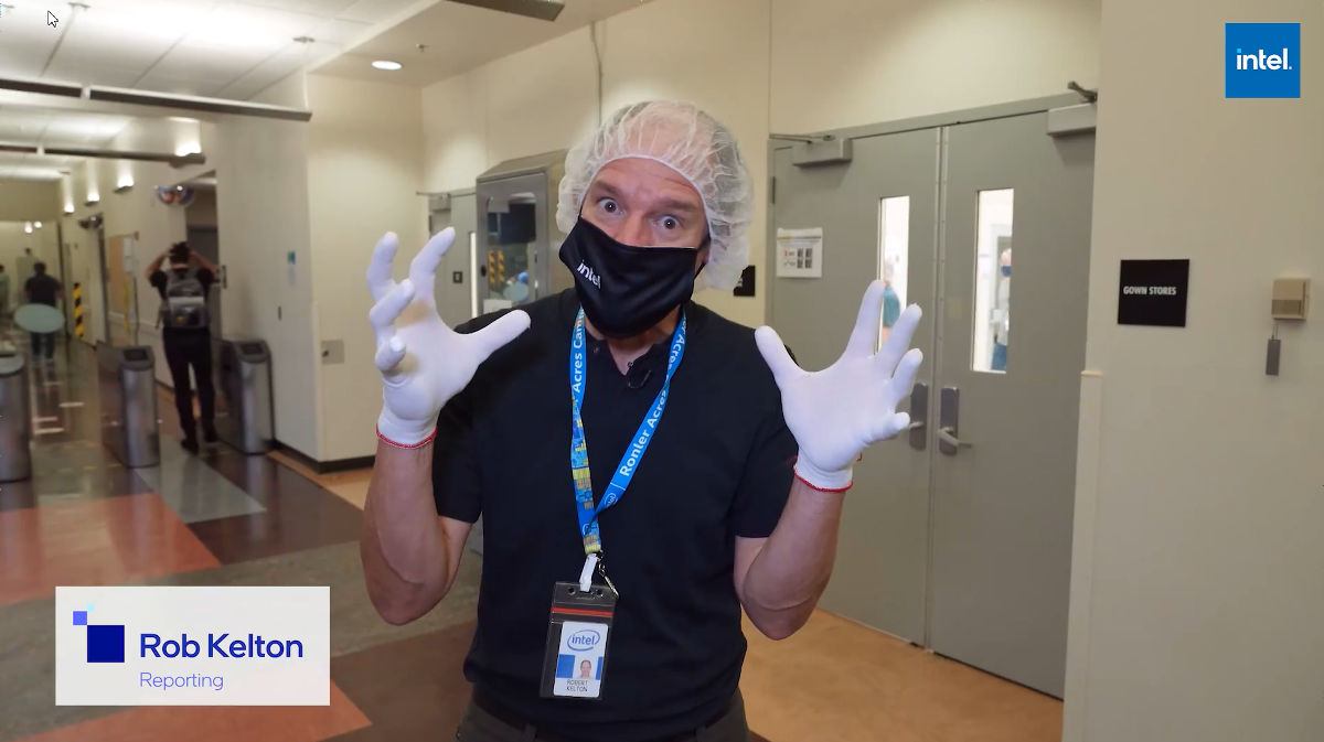
Where Kelton, who is fully defensive, heads for ...
'
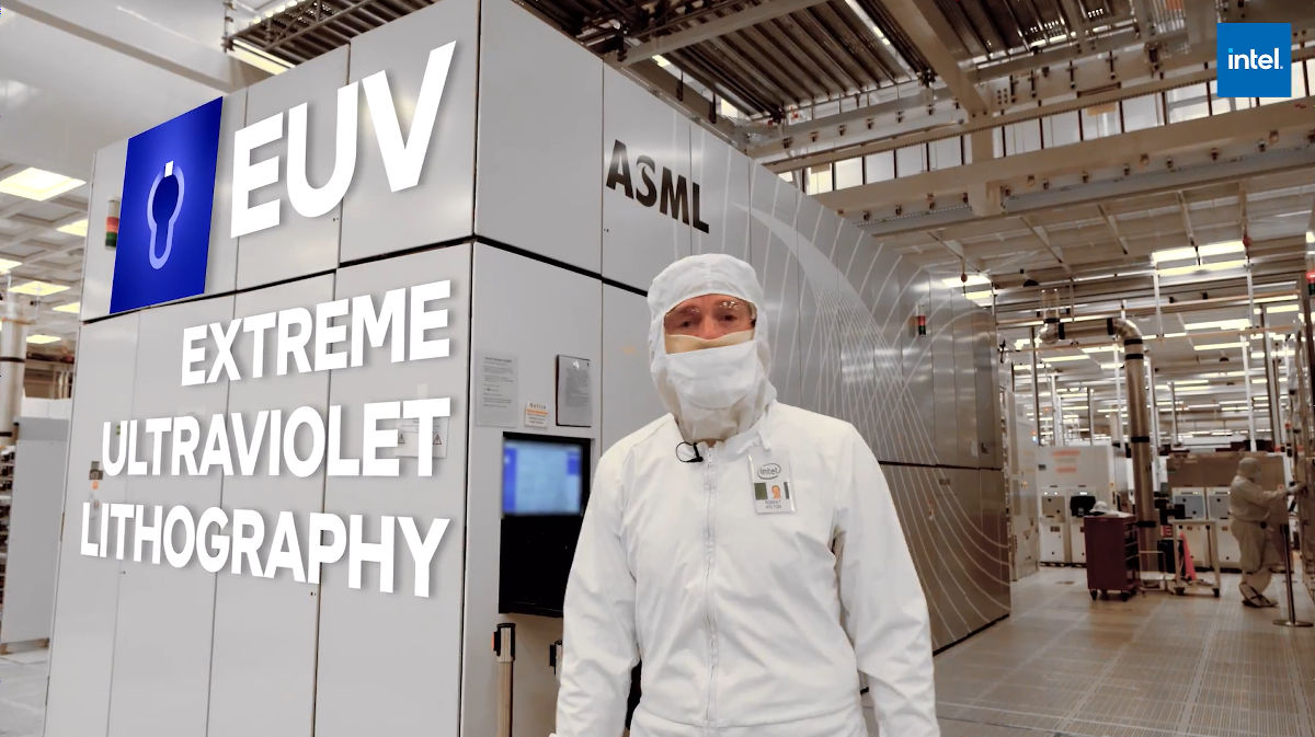
Kelton describes EUV as 'one of the most complex machines humans have built.' EUV is indispensable for chip manufacturing and promotes
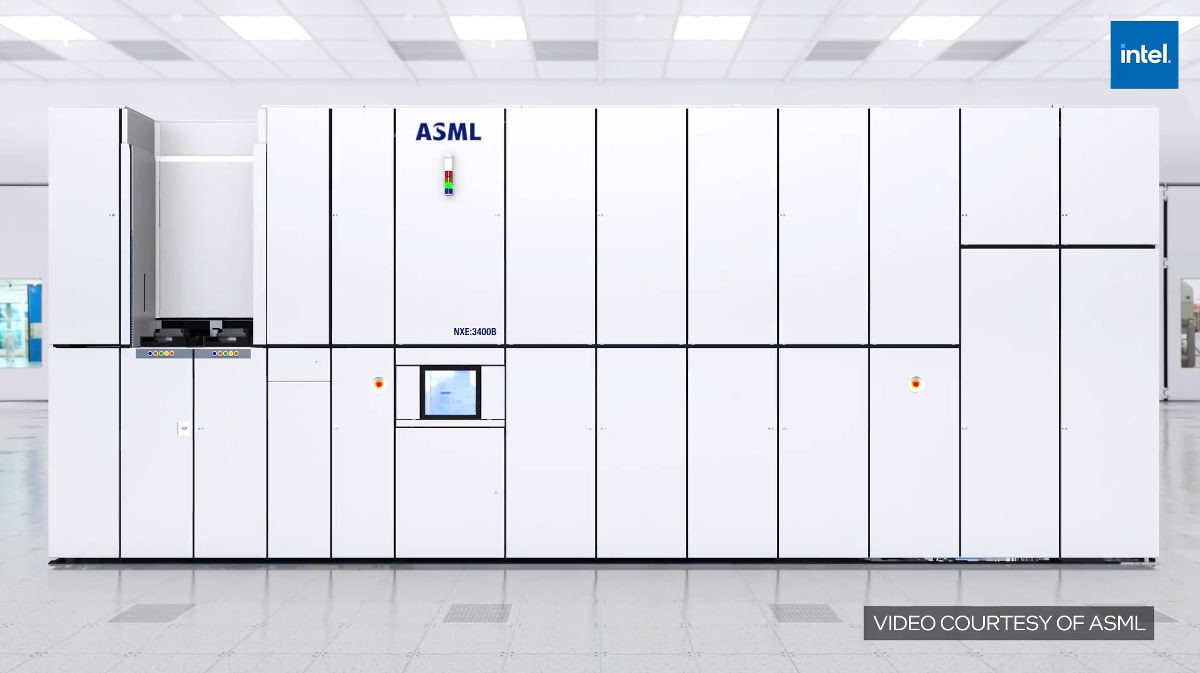
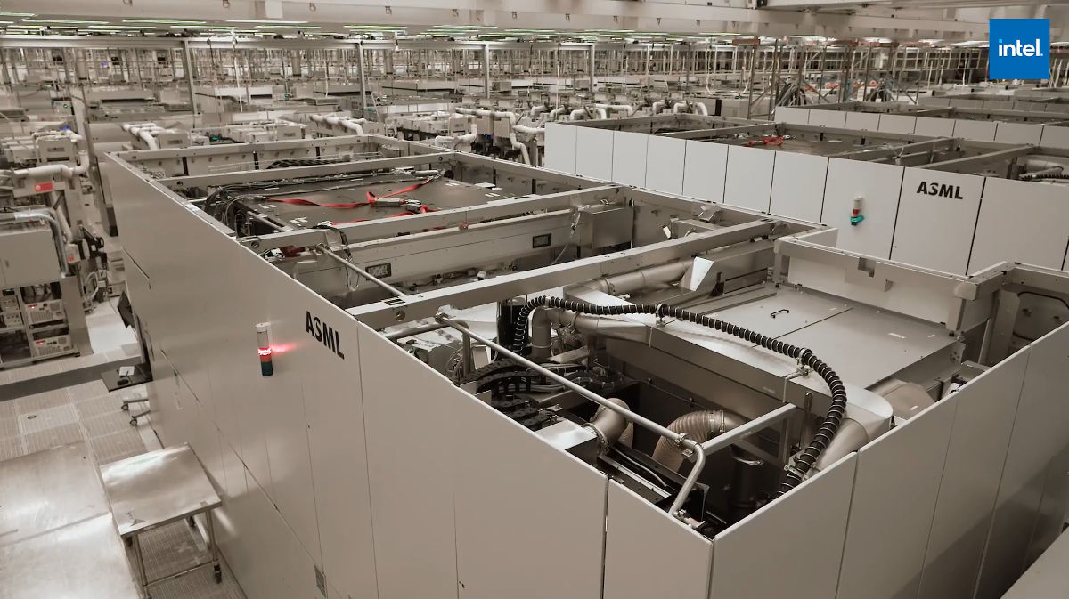
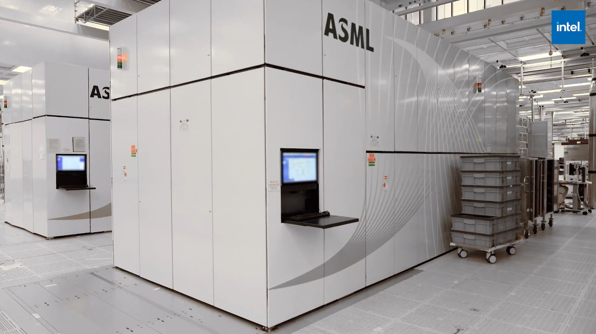
EUV was completed after 35 years of research by semiconductor manufacturers ASML , which leads the field of lithography (exposure equipment), and companies such as Intel, TSMC, and Samsung.
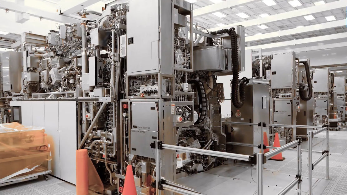
Seen from the side, it looks like this ...
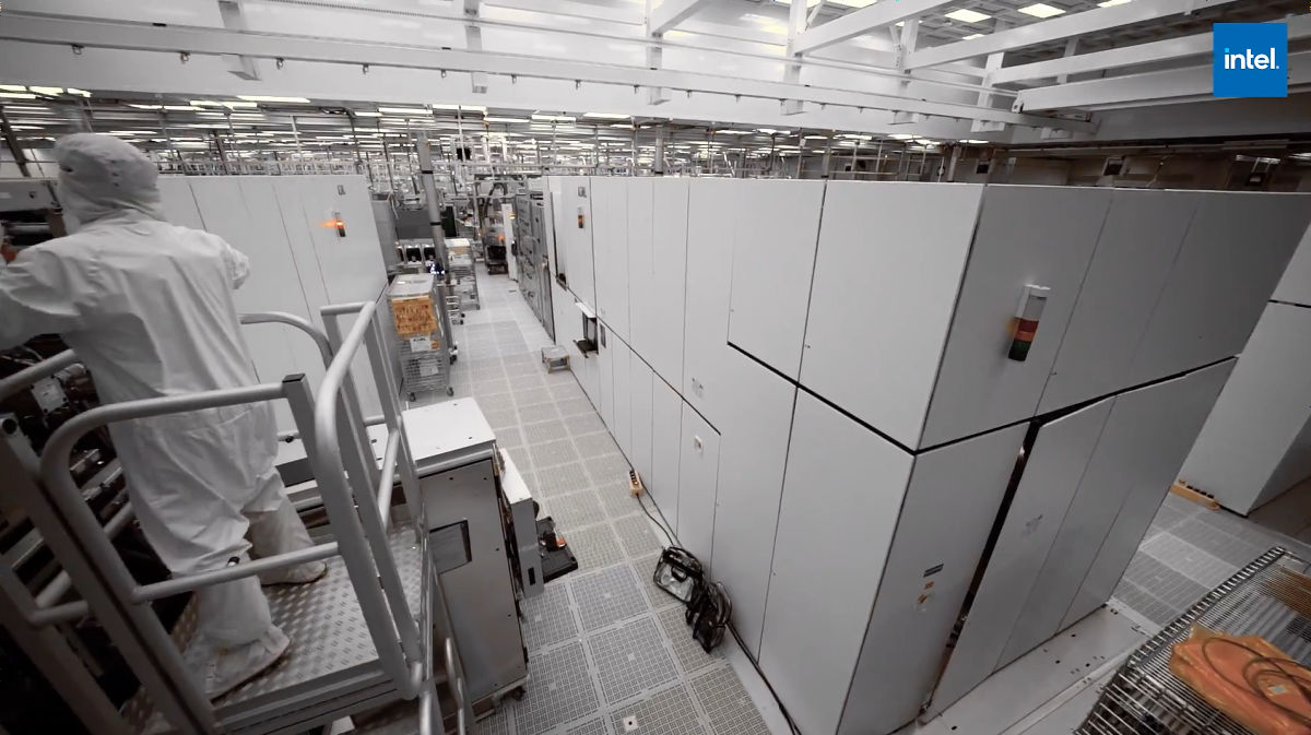
Here is the inside view.
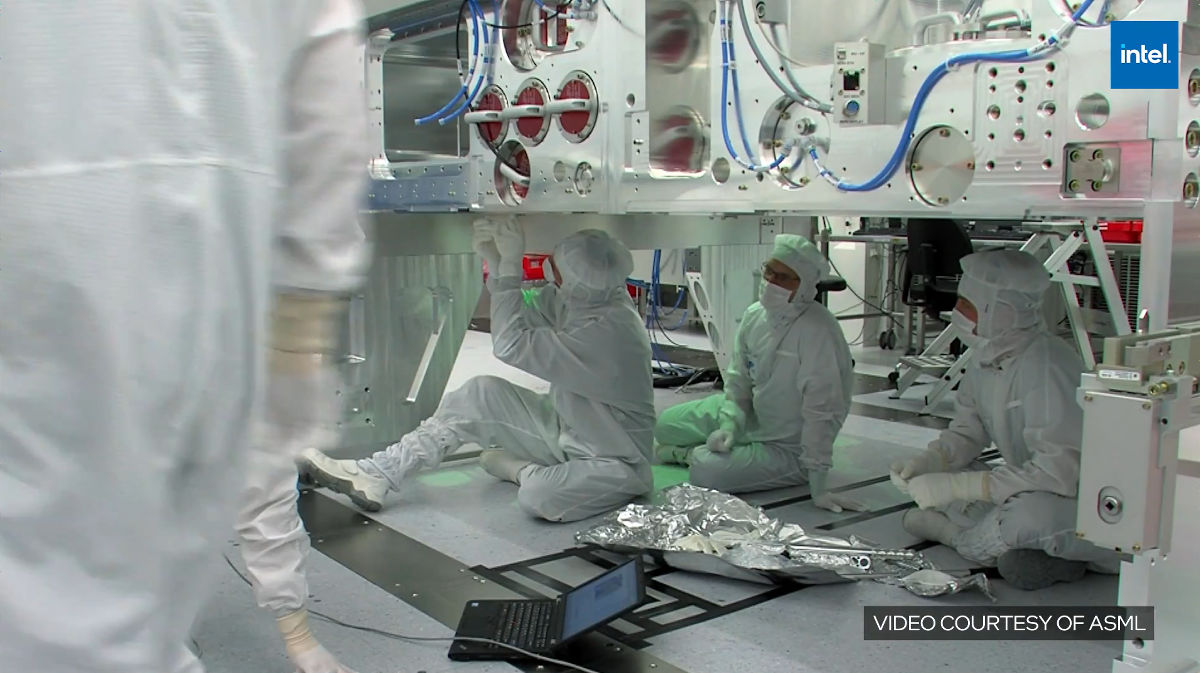
Three freighters will be used to transport EUV to
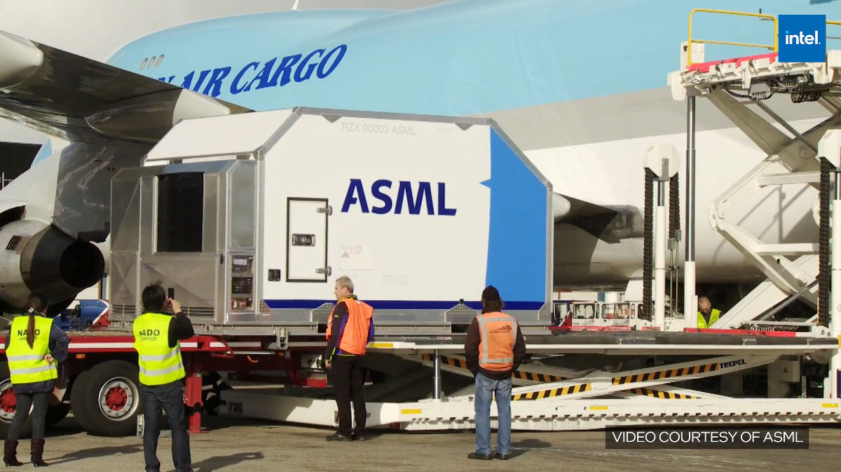
40 freight containers and 20 trucks are used.
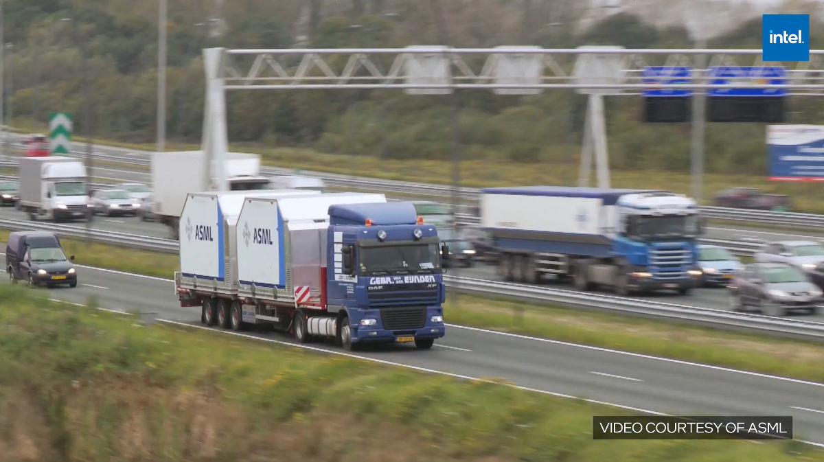
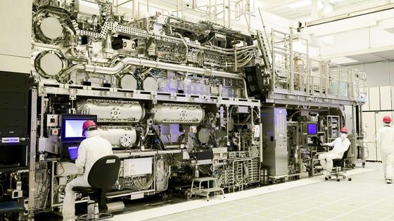
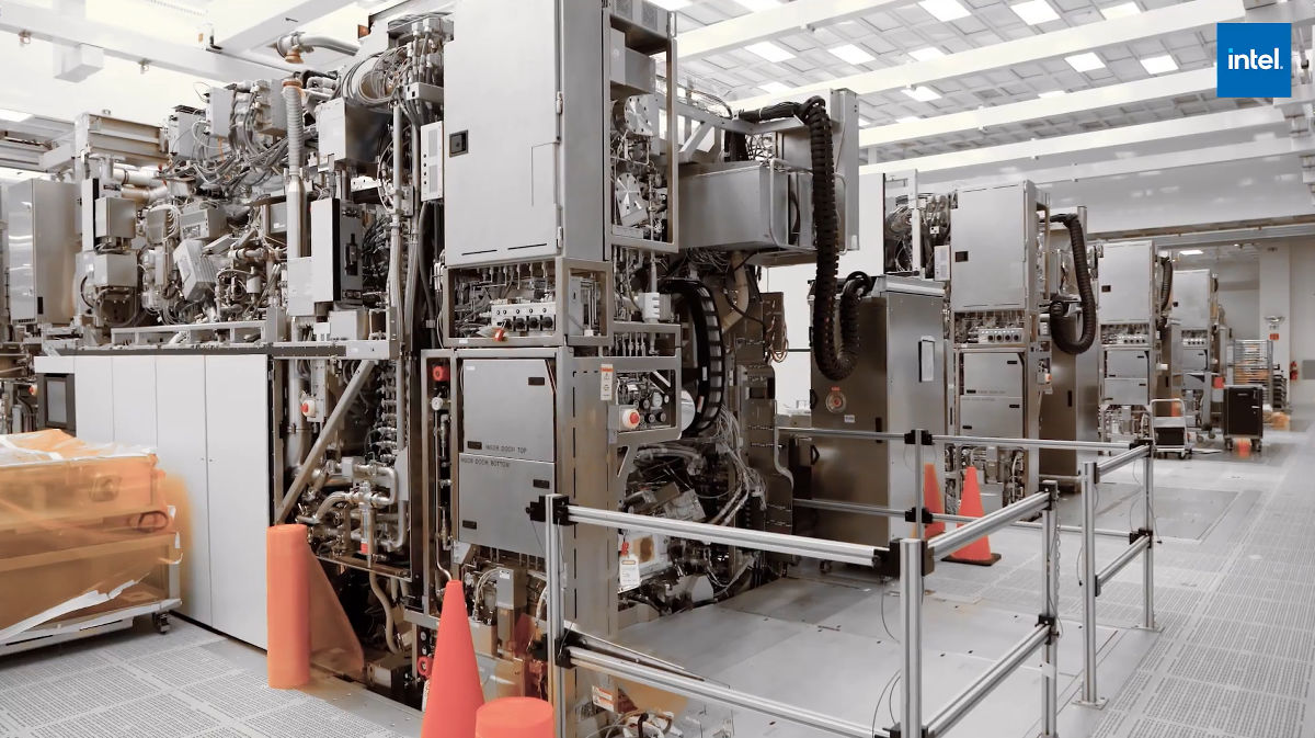
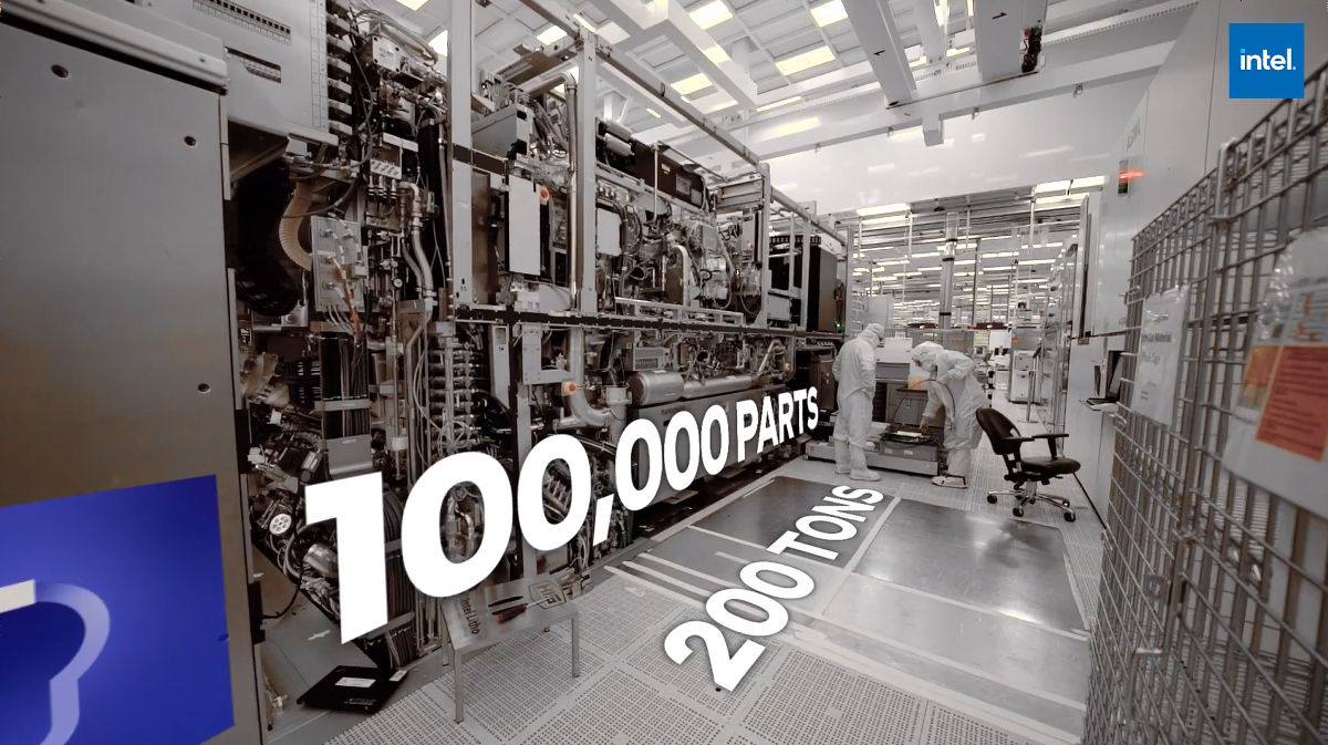
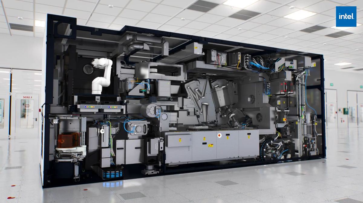
The EUV carried in this way is the size of a school bus, consists of 100,000 parts, and weighs 200 tons.
Intel co-founder
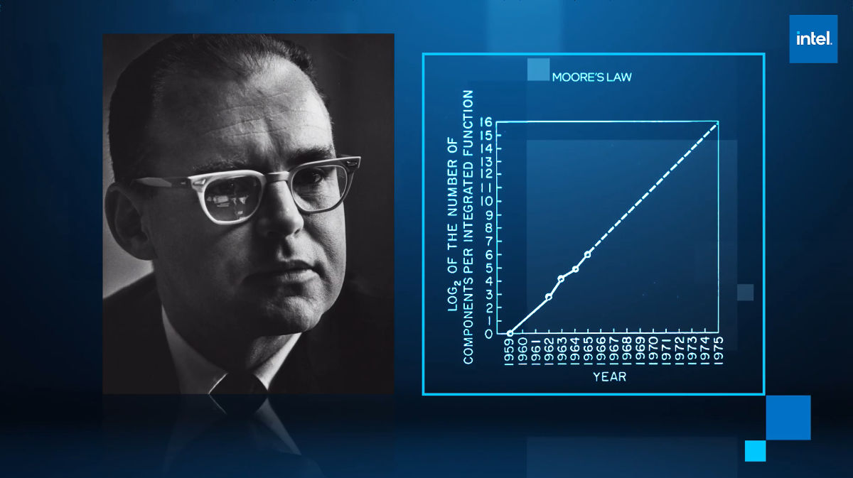
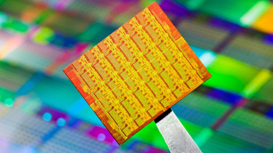
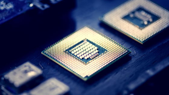
Transistors and components on chips continue to be stronger and cheaper.
Chip makers use lithographic machines to
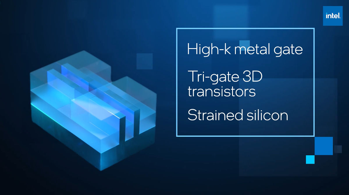
In pursuit of Moore's Law, Intel engineers developed what is called 'High-k metal gate Tri-gate 3D excluded Strained silicon'.
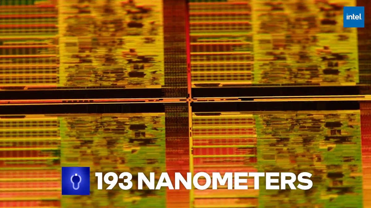
Intel and other manufacturers have also sought to reduce wavelengths by using multi-patterning (multiple exposure) processes such as 'double patterning' and 'quad patterning', as well as a method called immersion lithography.
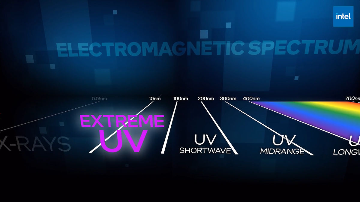
Through these efforts, the wavelength of light today has been reduced to 193 nanometers. However, in order to make the transistor smaller than this, the semiconductor industry thought, 'We need EUV that uses dramatically shorter wavelengths.'
The EUV system that appeared at the beginning was developed there. This system uses a wavelength of 13.5 nanometers, which is 10 times shorter than past machines.
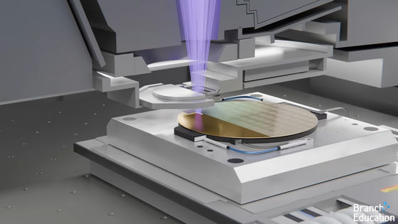
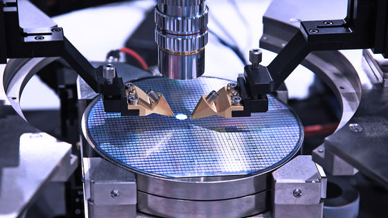
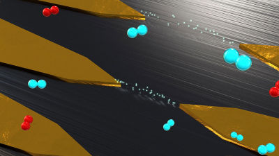
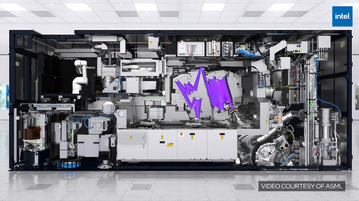
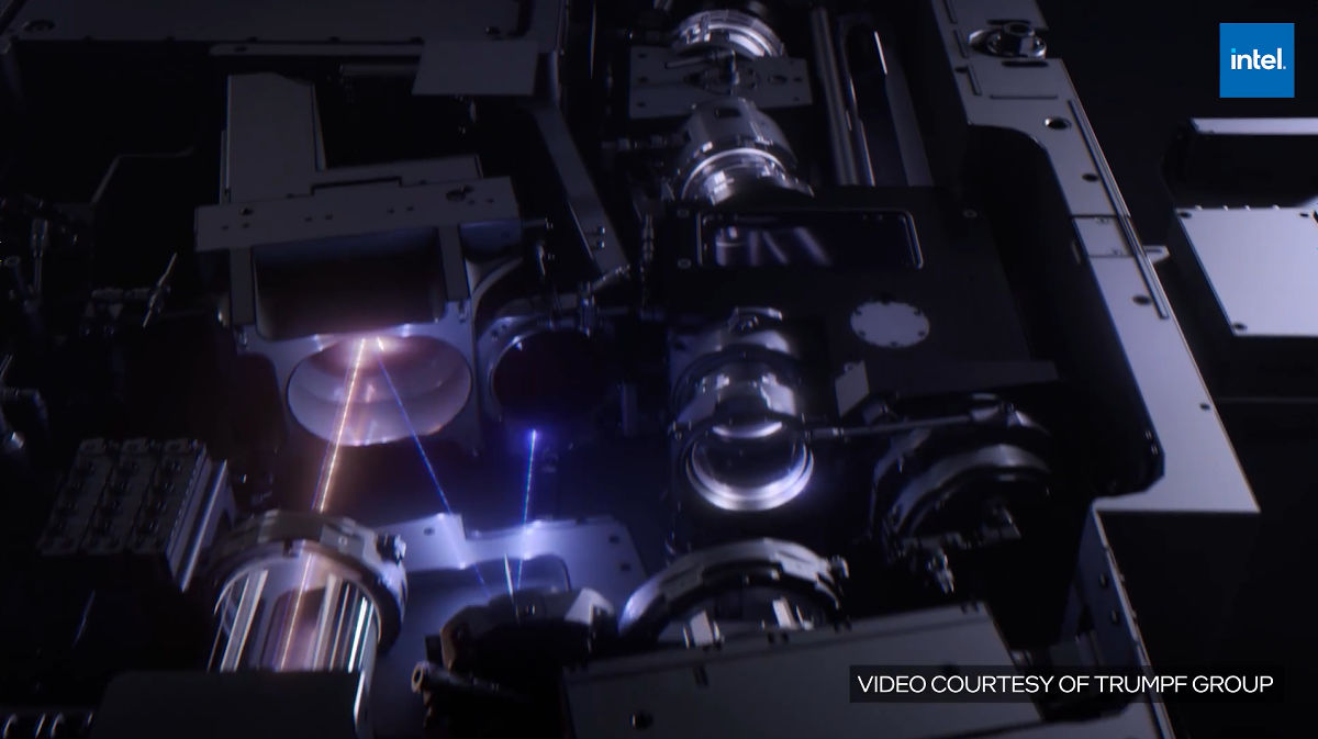
The function of the EUV system is as follows. First, as a premise, EUV uses what is called 'extreme ultraviolet rays' that does not exist in nature.
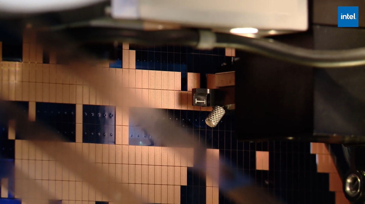
In addition to being huge, the EUV system also features a laser that is 15 times more powerful than the laser that cuts steel in Fab.
The mechanism is that the beam transport system first sends a laser pulse into the EUV machine.
Around that time,
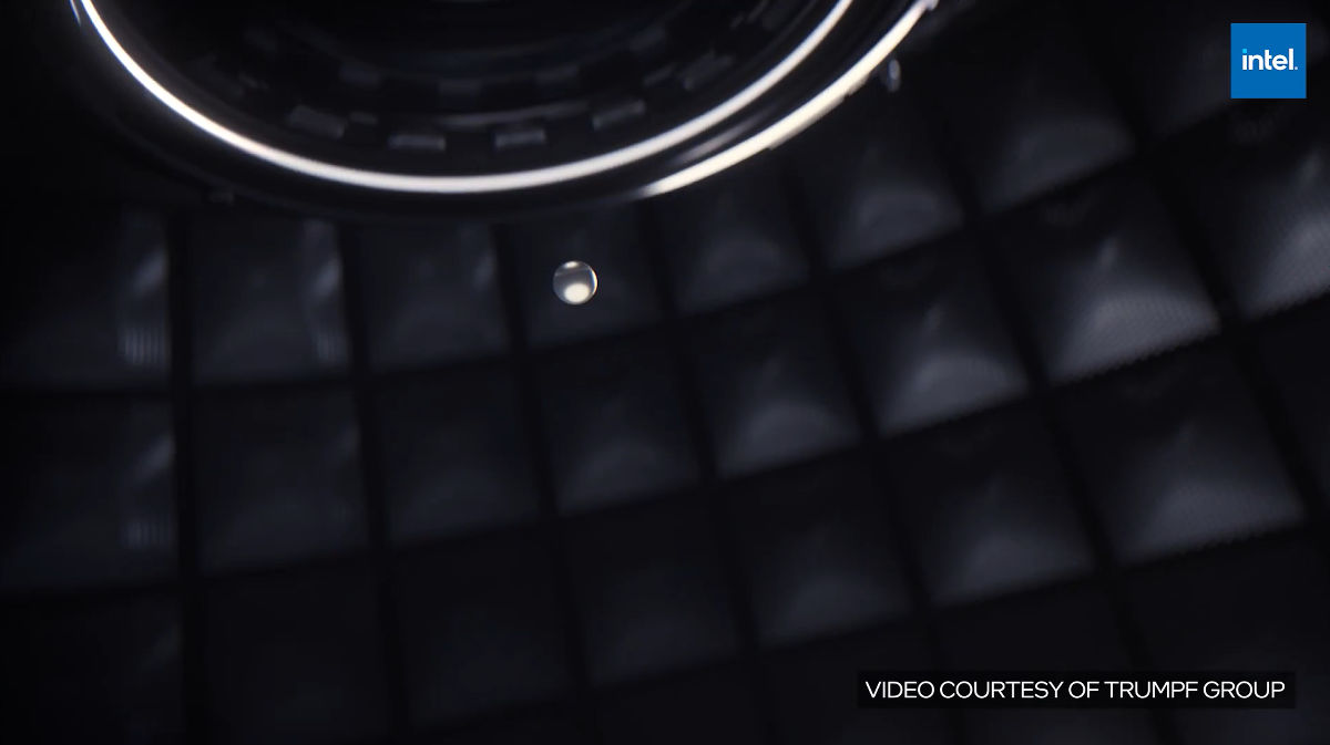
Then, a powerful laser irradiates the droplet 50,000 times per second. This vaporizes the droplets into plasma.
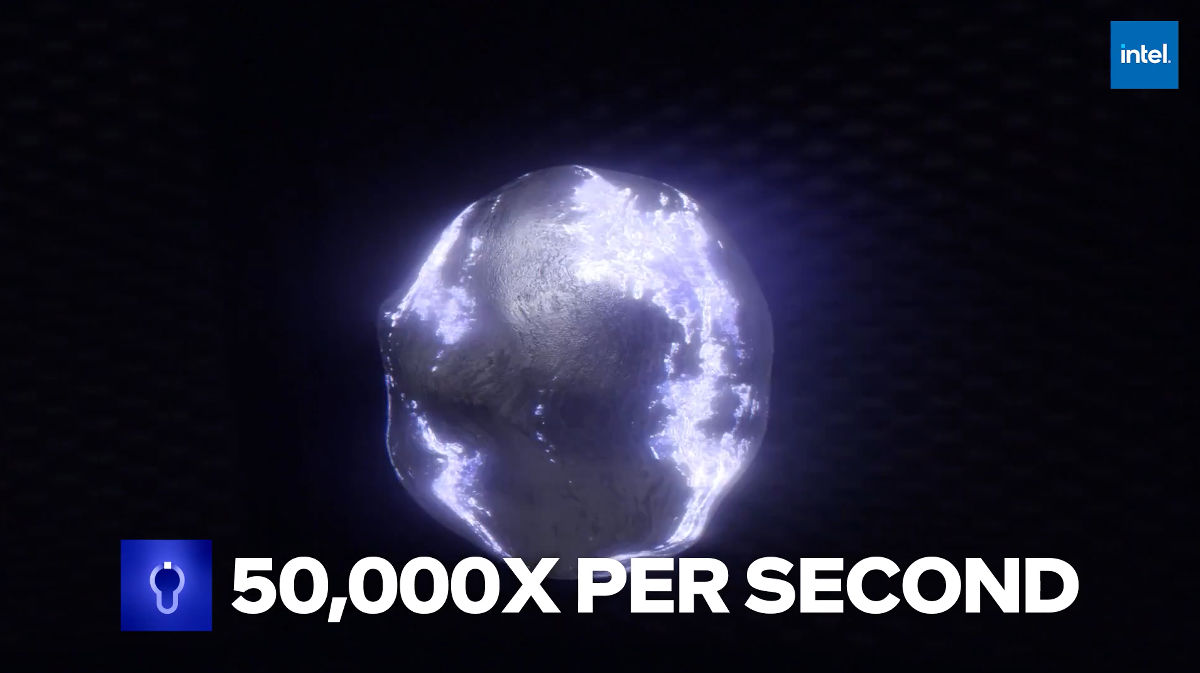
It is said that this plasma emits light at the wavelength of extreme ultraviolet rays.
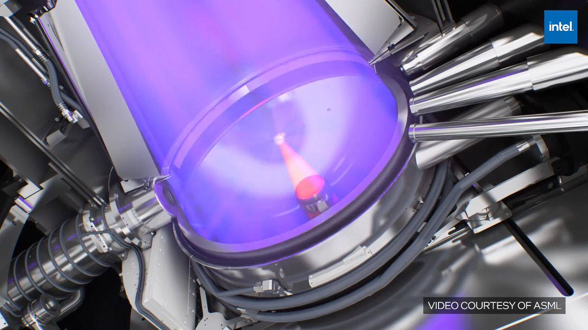
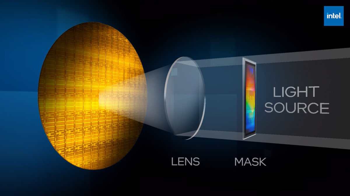
The condenser mirror collects EUV light with a wavelength of 13.5 nanometers.
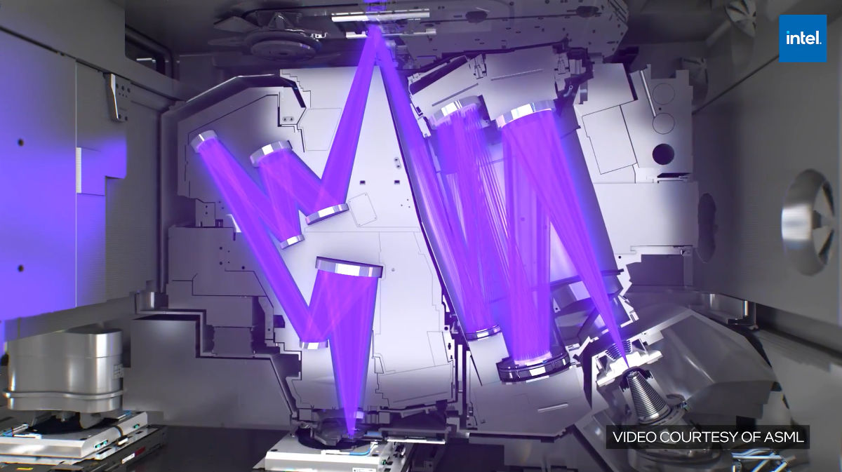
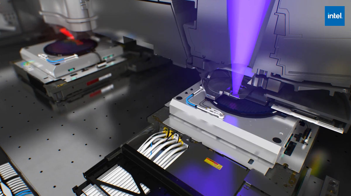
When the collected light is applied to the scanner, the scanner reflects the light like a mirror.
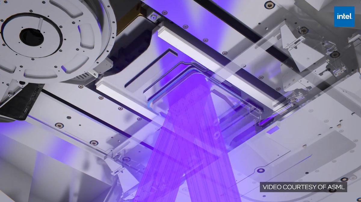
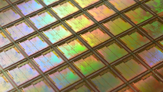
This reflection is used to create transistor patterns and interconnects on silicon wafers.
'How about it? It's simple,' says Kelton.
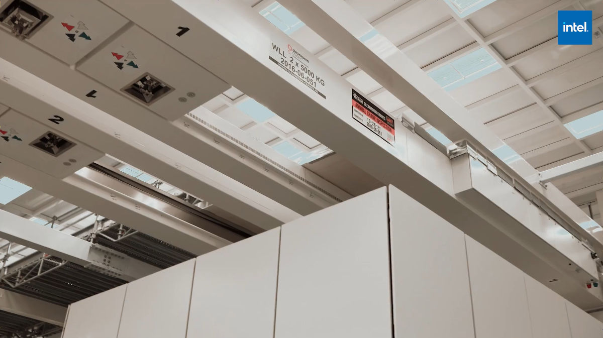
The feature of Intel's Fab with EUV is the ceiling height of 16 feet (4.87 meters).
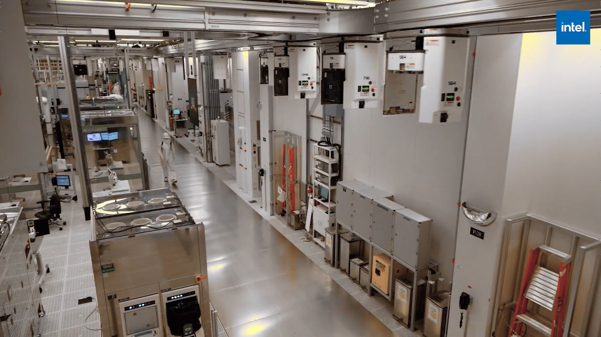
And you can raise it to 25 feet (about 7.6 meters).
This is because when assembling tall EUV, heavy parts need to be carried by a crane installed on the ceiling.
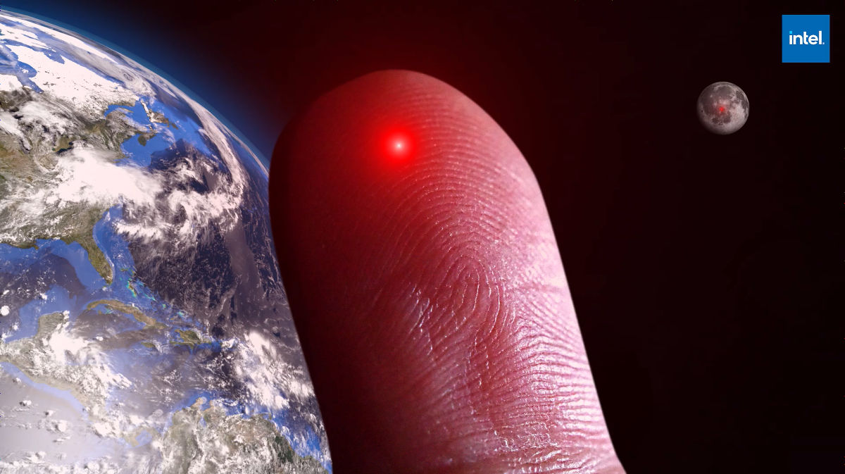
In addition, EUV needs to be as precise as 'an astronaut on the moon irradiates the thumb of a person on the earth with a laser pointer.'
Due to this precision, ASML is currently developing EUV tools on an ongoing basis.
Intel is the first customer to utilize ASML's EUV system as described above. In recent years, as 'Moore's Law is being celebrated the limit'
Related Posts: