What is Intel's next move to solve the semiconductor shortage and restore rights?
Intel CEO Pat Gelsinger said that the
Inside Intel's EUV chip manufacturing tech built by ASML --Protocol — The people, power and politics of tech
https://www.protocol.com/enterprise/intel-euv-fab-chips
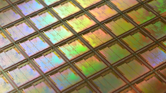
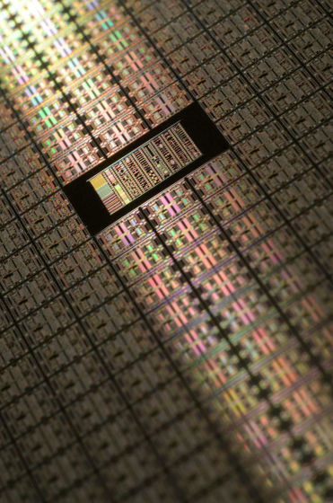
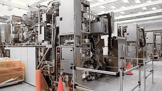
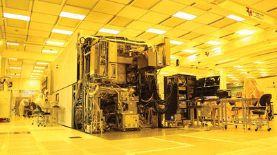
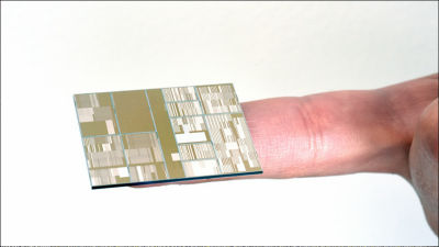
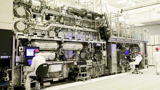
Intel's Lonler Acres Campus in Hillsboro, Oregon, USA, is a technological development base responsible for the design and development of mass-produced chips at manufacturing plants called fabs and foundries. And, in one corner, the equipment of 'extreme ultraviolet (EUV) lithography ' exclusively produced by the Dutch semiconductor manufacturing equipment manufacturer ASML is scheduled to be introduced in the near future.

EUV lithography is a technology that uses plasmatized
Intel plans to make a comeback in the semiconductor industry by responding to the prolonged shortage of semiconductors with EUV lithography, which can produce semiconductors with higher efficiency than before. Intel CEO Gelsinger often says at an event held by the company in the summer of 2021, 'I usually say,'It's easy to get second in the race, but it's hard to get first.'' And we're trying to catch up faster with less energy, which will be a big help to learn from ASML and deepen our relationship with ASML. ' I was motivated to reinstate.
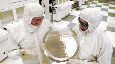
EUV lithography manufactured by ASML in the Netherlands is delivered to Intel's factory in thousands of parts. Lithography, which costs $ 180 million per unit, is 12 feet high and weighs about 180 tons when assembled. According to Intel's director of lithography, Mark Phillips, the EUV lithography vacuum chamber is too large to carry even a Boeing 747 as it is, so it will be airlifted in three parts.
Under EUV lithography, a variety of equipment is installed, including transformers, power conditioners, vacuum pump racks for hydrogen removal equipment systems, and CO2 driver laser power racks used to plasmat tin. This CO2 driver laser was originally developed by a laser company called Trumpf for cutting metal, and among them, four particularly powerful laser devices are combined into one and diverted for EUV lithography. Philips commented on the struggle to implement EUV lithography: 'It was incredibly difficult to emit a 13.5 nm ray with enough power to expose a photoresist. To develop this light source, The entire industry has been stagnant for several years. '
Intel has reigned at the top of the semiconductor industry for many years, but in recent years AMD has lost its share in areas such as consumer chips, and technical delays have become noticeable. 'Intel's delay was due to EUV not being ready when we tried to move to 10nm technology,' said Sanjay Natarajan, Intel's co-general manager of technology development. He showed the idea of gaining momentum to regain the market share by introducing EUV lithography this time.
According to Natarajan, Intel's next-generation chip with EUV technology will be available in 2023, first on the market as a 'Meteor Lake' chip for desktops and a 'Granite Rapids' chip for servers. That thing. 'EUV technology will be at the forefront of chip manufacturing technology for at least the next decade,' said Natarajan.
Related Posts:
in Note, Posted by log1l_ks