What is the expected manufacturing technology "EUV lithography" that can avoid the limit of "Moore's Law"?
"Moore's Law" which predicted the growth rate of semiconductor innovation that "semiconductor integrated circuit density doubles every two years"It will end in the near futureIt is said. Gordon Moore, one of the founders of Intel who advocated this law, also states that "transistors are small and reach their limits to the atomic level", but major semiconductor makers say "EUV lithography"We are promoting the practical use of it, and within the next few years the possibility of being able to avoid the limit of Moore's law is emerging.
Leading Chipmakers Eye EUV Lithography to Save Moore's Law - IEEE Spectrum
http://spectrum.ieee.org/semiconductors/devices/leading-chipmakers-eye-euv-lithography-to-save-moores-law
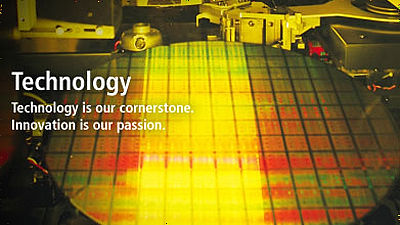
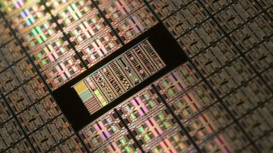
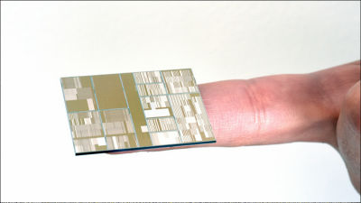
The width of the wiring when manufacturing the semiconductor circuit on the wafer is called "process rule" and the CPU is classified as "14 nm generation" or "22 nm generation" depending on the minimum processing size, but the next generation "10 nm generation "Development is significantly delayed, Intel 's 10 nm process adoption product" Cannonlake "will also appear in 2017 is expected to be. Therefore, as a technology for manufacturing state-of-the-art processors,EUV lithographyIf technology called so called is put into practical use, development schedule based on Moore's law is seen to be established.
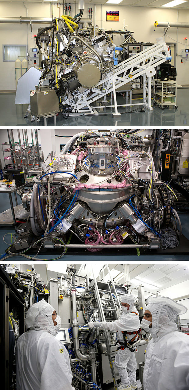
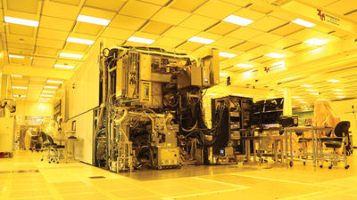
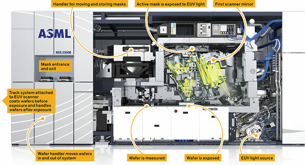
EUV lithography is a lithography technology using extremely short wavelength laser beam called extreme ultraviolet ray, which enables semiconductor processing with dimensions of 20 nm or less, which is difficult to process with conventional technology, and if integrated, the density of integrated circuit parts It is said to be more than double. EUV light with a short wavelength of 13.5 nm can obtain sufficient brightness (intensity) by extracting it from the plasma, which is more practical and more economical than using X-rays or particle accelerators.
To put EUV lithography lasers into practical use, it is necessary to maintain output of 250 watts or more, but in the beginning of 2016, the semiconductor manufacturers in the Netherlands ·ASMLAlthough it is a laboratory environment, we report that we achieved output of 200 watts using pre-pulse method.
The incorporation of EUV lithography in the production line is approaching a not-so-distant future, and in 2018 Intel and TSMC have the promise of putting EUV lithography into practical use. GlobalFoundries plans to manufacture the "7 nm generation" in 2018 without EUV lithography, but it is planning to incorporate EUV as soon as preparation is completed. Furthermore, TSMC will adopt EUV lithography in 2020 for the production line of "5 nm generation".
Related Posts:

in Hardware, Posted by darkhorse_log