IBM expects to overcome the 10 nm generation and succeed in prototyping a 7 nm process semiconductor chip and to adhere to Moore's Law
IBM will enable world's smallest semiconductor chip manufacturingManufacturing process(Process · Rule) It became clear that trial manufacture of 7 nm chip was successful.
IBM Discloses Working Version of a Much Higher-Capacity Chip - The New York Times
http://www.nytimes.com/2015/07/09/technology/ibm-announces-computer-chips-more-powerful-than-any-in-existence.html
Beyond silicon: IBM unveils world's first 7 nm chip | Ars Technica UK
http://arstechnica.co.uk/gadgets/2015/07/ibm-unveils-industrys-first-7nm-chip-moving-beyond-silicon/
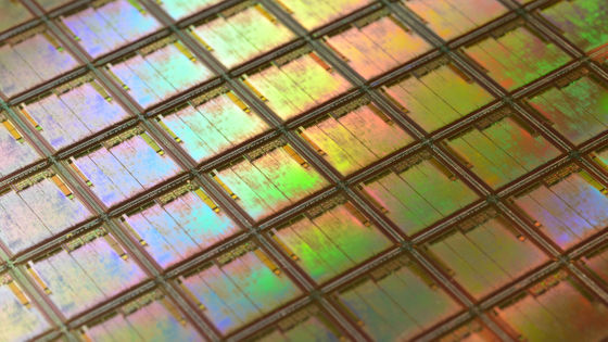
Wiring width when manufacturing semiconductor circuits such as CPU and memory on a wafer is called process rule and is called "14 nm generation" or "22 nm generation" depending on the minimum processing size. As generations advance and minimum processing dimensions become smaller, it becomes possible to place more transistors and wirings on the same area, so it is thought that further speeding up of semiconductor can be realized.
Intel founder Gordon Moore advocated, "The number of transistors on an integrated circuit doubles every 18 months" famous "Moore's lawSo far, semiconductor circuits have been improving the performance by increasing the density of integrated circuits on wafers.
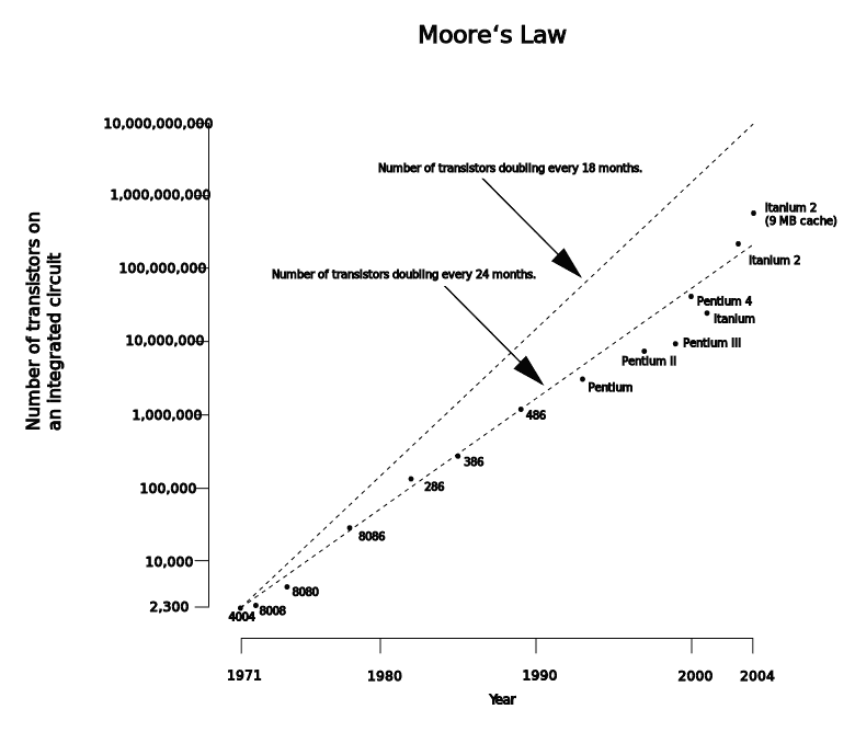
At the moment, the prosel rule of the most advanced semiconductor chip which is put into practical use is 14 nm generation, and semiconductor miniaturization technology is being enhanced for the practical application of 10 nm process as the next generation chip, but Intel And TSMC and others are the "limit theory of miniaturization technology" to be heard, the development of microfabrication technologies after the 10 nm process has been difficult and there was concern that Moore's Law would not hold in the future It was.
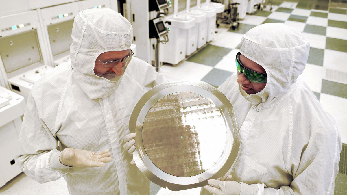
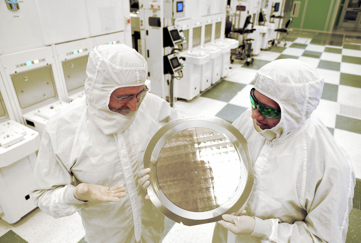
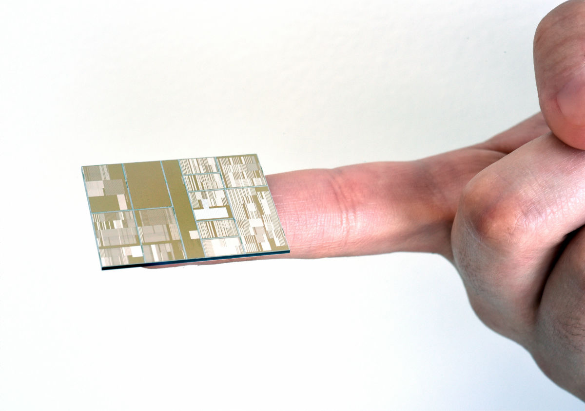
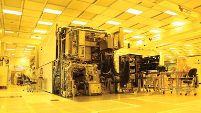
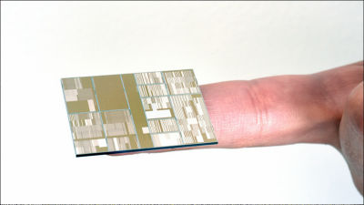
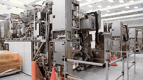
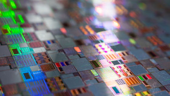
Meanwhile, IBM cooperated with GLOBALFOUNDRIES, Samsung, etc., it became clear that the world's first successful prototype chip of 7 nm process. IBM said that it adopts silicon germanium instead of pure silicon for the material of the switching part of the molecular size FinFET. For wafer masking / exposure,Extreme ultraviolet lithography (EUV)It is expected that the technology is used.
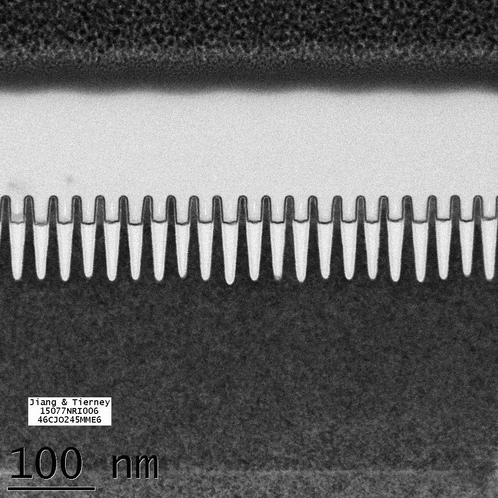
Although it is not possible to pin how small the minimum processing dimension of 7 nm process is, the diameter of erythrocytes in the blood is about 7500 nm and the diameter of the chain of DNA is about 2.5 nm, so the awkwardness of miniaturization technology in semiconductor chip circuit design It is transmitted.
The chips that adopted the 7 nm process that IBM successfully trialized are expected to be marketed from 2017 to 2018, and until February 201 Moore's law is likely to be maintained. The giant IBM seems to have given the giant IBM to the chip development competition of 10 nm or later against Intel which leads overwhelmingly the semiconductor market for PC and Qualcomm, TSMC, Samsung which pulls the development of chip for mobile terminal.
Related Posts:


in Hardware, Posted by darkhorse_log