Intel technical executives talk about Intel's revised process rules and new roadmap
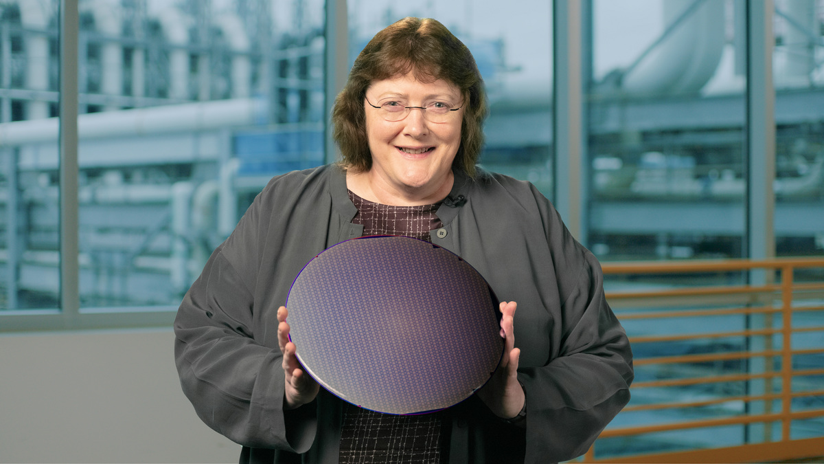
In an interview with Semiconductor Engineering, a semiconductor-related news site, Intel's senior general manager of technology development, Ann Kelleher, talks about Intel's future roadmap.
Inside Intel's Ambitious Roadmap
Semiconductor Engineering (SE):
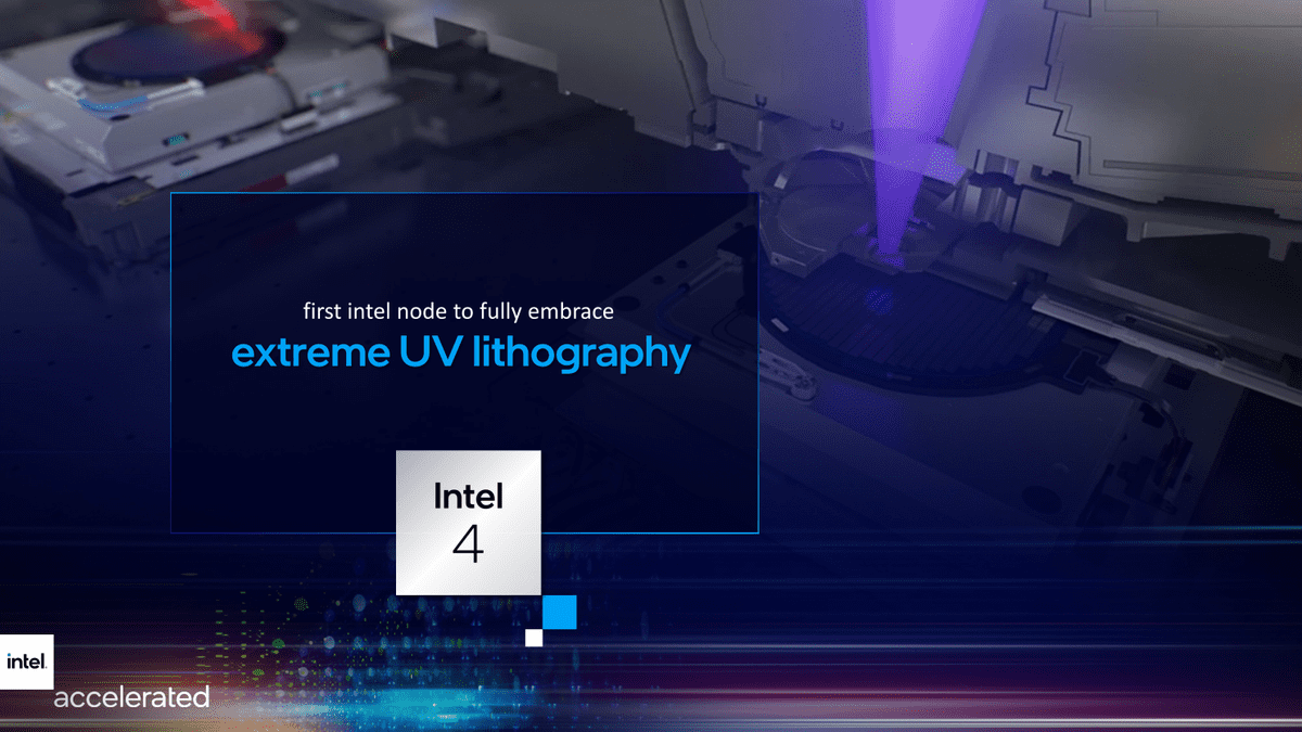
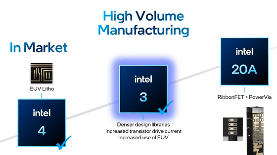
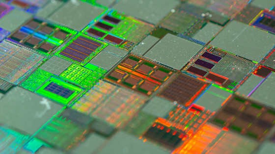
Intel published a roadmap to 2025 in July 2021. The conventional process node has also been renamed to 'Intel 7', 'Intel 4', and 'Intel 3', and the 'Intel 20A', which exceeds 'Intel 3', has been announced.
Intel announces partnership with Qualcomm to manufacture new chips, reveals roadmap to 2025-GIGAZINE

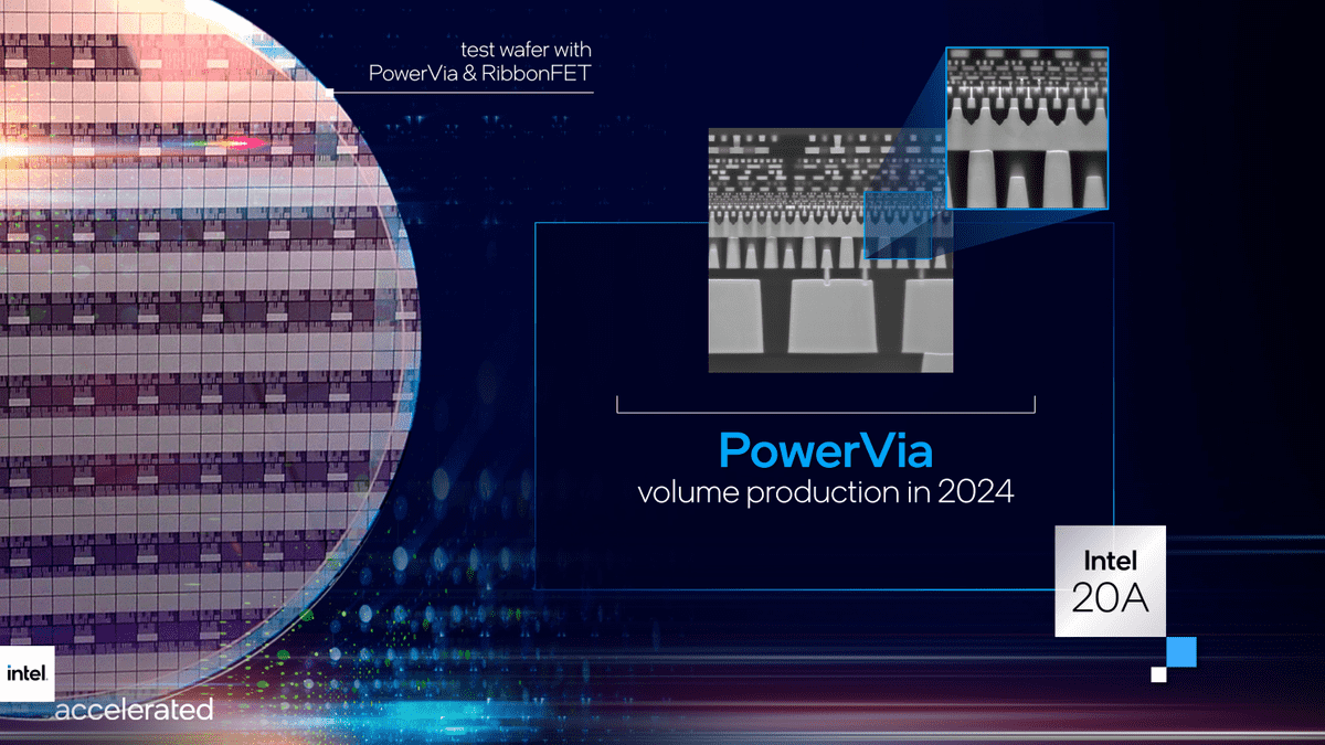
It is said that this Intel 20A will implement 'Ribbon FET', which is a new architecture of field effect transistor (FET) . What is Ribbon FET in the first place?
Mr. Anne Kelleher (hereinafter referred to as Mr. Kelleher):
RibbonFET, which is called by Intel, is called 'gate all-around structure' in the industry, and is a next-generation transistor architecture that surpasses FinFET. FinFETs will be improved up to Intel 3, but Intel 20A plans to use Ribbon FETs with process nodes that are almost the same as those of other companies.
SE:
When it comes to FinFETs, Intel has made a lot of progress. RibbonFET is a state-of-the-art node that will bring the industry forward again. Is it possible to realize Ribbon FET using current
Mr. Kelleher:
The Intel 20A, planned for 2024, uses existing EUV lithography with a numerical aperture (NA) of 0.33 for the exposure system. We have already partnered with ASML to use next-generation high NA EUV lithography for processes after 2025. Next-generation high NA EUV lithography allows you to move to much smaller shapes, much smaller pitches, and even continue to use double patterning technology.
We were interested in high NA EUV lithography a few years ago, and from around 2018 we were talking with ASML about 'what to do next'. In short, it's a goal that the industry as a whole needs to aim for. Therefore, the goal set by Intel for 2025 is the adoption of next-generation high NA EUV lithography. EUV lithography was not introduced in our 10nm process, Intel 7, but it is introduced in Intel 4. We want to stay on the cutting edge of EUV lithography.
SE:
Intel adopts FinFET up to Intel 3, and adopts Ribbon FET, that is, a gate all-around structure transistor after Intel 20A. Meanwhile, competitor Samsung has adopted gated all-around transistors in the 3nm process. Why didn't Intel adopt Ribbon FET in Intel 3?
Mr. Kelleher:
We knew that we could further improve the FinFET roadmap in terms of the original optimization. So why not take advantage of these benefits before moving to a completely different architecture? The point is, 'When is the right time to do it?' We move on the belief that Ribbon FETs can basically provide more than existing FinFETs. It will be clear at some point how other industries will introduce gate-all-around structures.
SE:
Several companies have long been working on gate-all-around transistors. What are the challenges with this technology?
Mr. Kelleher:
In the last few years, EUV lithography technology has matured significantly and has been fully adopted. Until now, the question was whether EUV lithography could handle all layers, but the printing process for EUV lithography has also become significantly easier. EUV lithography plays an important role in achieving a gate-all-around structure. In addition to these problems, the height and the substrate of the stack insulation separation you also have to think about what to do with the (isolation). It's all an issue to be addressed, but we know the path to solving all of these and delivering on time while reducing shortcomings.
SE:
Why did Intel rename the process node in the first place?
Mr. Kelleher:
In short, there was a gap in the names of nodes throughout the semiconductor industry. A Google search reveals that 'Intel's 10nm is equivalent to 7nm in other foundries.' We had to think about making it easier for our customers. After changing the node naming strategy, customers can finally make better decisions by looking at process nodes and their names.
We announced the vision for IDM 2.0 in March and have spent a lot of time creating a very detailed roadmap for the next six months.
Intel announced 'IDM 2.0' aiming to expand foundry services by investing more than 2 trillion yen, and it was pointed out that 'I am planning to manufacture Apple Silicon' --GIGAZINE
The new roadmap shows how to be able to take leadership in performance per watt, alongside other companies in performance per watt. In such a situation, we thought it was time to change the name. We spend more time focusing on what we're doing rather than explaining the names of the nodes.
SE:
It was said that Intel's 7nm process technology was lagging behind. What's happening now?
Mr. Kelleher:
As announced, what was then called the 7nm process is now called Intel 4. At the time of the name change, we reset the milestone once based on the development of the entire process and the defect density. Then, in order to streamline the process flow, we increased the adoption of EUV lithography while basically proceeding with the old process flow and the new process flow in parallel. As a result, we were able to switch from the original process flow to the new process flow in 2021. This new process flow is working very well.
We have achieved milestones in the last nine months and are confident that the work we are doing is paying off. We also talked about how to put together a roadmap to lead the industry in performance per watt. First, we plan a considerable number of projects and invest R & D and capital to realize them. And Intel's technology development group has world-class engineers. It has been and is still the case. But the way we work is changing. We adopt industry standards wherever possible and wherever it makes sense.
SE:
Intel plans five nodes over a four-year period, aiming to be a leader in the industry, alongside its competitors. This overturns the previous rule of 'announce new process nodes every 18 to 24 months', right?
Mr. Kelleher:
We will release Intel 7 products in late 2021. And Intel 4 will be commercialized in the latter half of 2022 and will be on the market in 2023. Intel 3 will be available in late 2023. The Intel 20A will follow in 2024, followed by the Intel 18A. Performance per watt when migrating to the next node will all improve significantly. But if you want to catch up with or go beyond your competitors, your chips need to move faster. The methodology I've talked about here is to make that possible. We have a very solid roadmap to achieve this.
Related Posts:

in Hardware, Posted by log1i_yk