What is the next wave of 'Moore's Law' that Intel thinks?
'Moore's Law' states that 'the integration density of semiconductors will double in 18 to 24 months, and even if the performance of chips doubles, further miniaturization will proceed', Gordon, one of the founders of Intel Moore predicted the future in 1965.
Intel's Take on the Next Wave of Moore's Law - IEEE Spectrum
https://spectrum.ieee.org/whats-next-for-moores-law
According to Mr. Kelleher, 'Moore's Law' refers to 'increasing the degree of integration of functions', which is equivalent to ' optimization of system technology (STCO) ' in the next 10 to 20 years. About. From the workload that the product should support and its software, to the system architecture, the silicon required in the package, and the semiconductor manufacturing process, we will develop outside-in methods that consider solutions based on the needs of society and customers. By doing so, ``we will optimize all the elements so that we can get the best answer in the final product,'' says Kelleher.
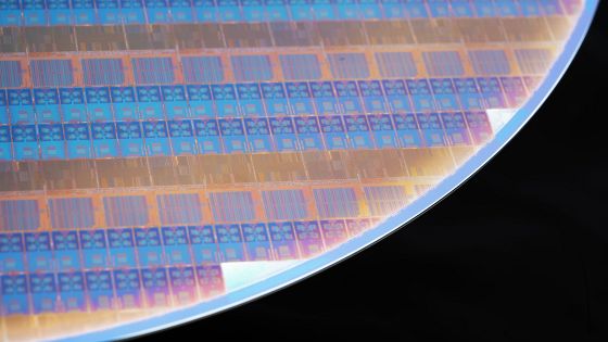
STCO has become an option because it divides functions that were previously contained in a single chip into small functional chips, chiplets, each of which is manufactured using the most suitable semiconductor process technology, and is capable of achieving high bandwidth. Being able to connect is a big factor.
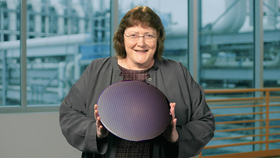
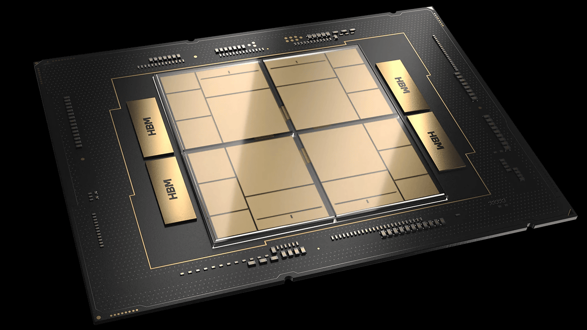
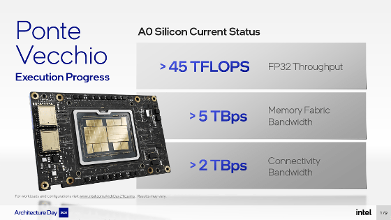
As a practical example of STCO, Mr. Kelleher mentioned the Ponte Vecchio processor , which is the heart of the supercomputer 'Aurora'. The Ponte Vecchio processor consists of 47 active chiplets and 8 thermally conductive blanks, connected by advanced 2.5D packaging technology and 3D stacking.
Intel announces details of game image quality improvement technology 'XeSS' and next-generation processor 'Alder Lake' - GIGAZINE
At
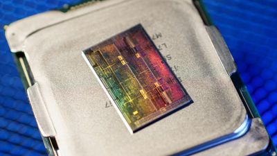
Kelleher pointed out that interconnect technology will be the biggest change in future semiconductor process technology. Intel plans to introduce a technology called 'PowerVia' in 2024. PowerVia will move the chip's power delivery network below the silicon, reducing logic cell size and reducing power consumption.
STCO is still in its early stages, and the electrical circuit design (EDA) tool is working on STCO's predecessor, 'design technology optimization (DTCO),' which is optimized for logic cell level and functional block level. It is said that emphasis is placed. Mr. Kelleher said, ``In the future, attention will be focused on methods and tools to realize STCO.''
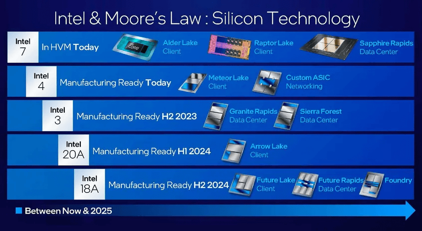
Kelleher's new Intel roadmap looks like this. The new transistor architecture RibbonFET and PowerVia will be introduced in the `` Intel 20A '' scheduled to be manufactured from the first half of 2024. Mr. Kelleher, who was asked about the risks of the new technology, answered, ``I think there is a big advantage because we can realize RibbonFET technology by moving to PowerVia.'' It seems that PowerVia's test using FinFET, which is a conventional architecture, was going well and was able to accelerate the development work.
Regarding the future of transistors, the design of planar transistors survived from 1960 to around 2010, and its successor, FinFET, is still alive. I think that it will be laminated at some point.”
Related Posts: