Intel completes development of process rules 'Intel 20A' and 'Intel 18A' aiming for industry leading edge

by
Intel has reportedly completed development of the Intel 20A and Intel 18A, which will be used to manufacture chips for its own products and customers of the Intel Foundry Services division. Intel 18A was supposed to be adopted after 2025, but it is said that it will be brought forward to the latter half of 2024 due to smooth development.
British Special Power Station Power Station Breakthrough in 2nd America R&D |
https://money.udn.com/money/story/5612/7009627?s=31
Intel Completes Development of 1.8nm and 2nm Production Nodes | Tom's Hardware
https://www.tomshardware.com/news/intel-completes-development-of-18a-20a-nodes
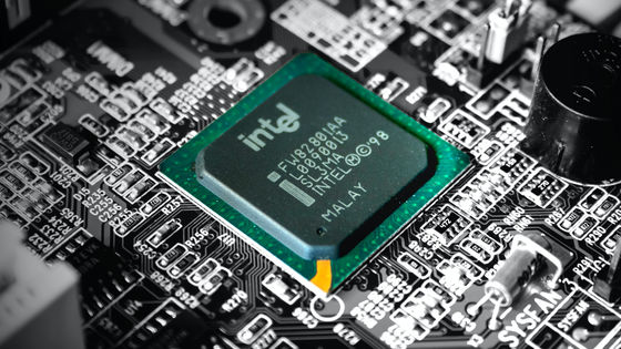
Process rules indicate the width and spacing of circuits on a chip, and the more advanced the process, the smaller the width and spacing of circuits. As the process rules become finer, the number of transistors that can be mounted on the same area increases, and the power efficiency and yield rate also improve.
Intel was lagging behind TSMC and Samsung, but in 2021 CEO Patrick Gelsinger announced a strategy `` IDM 2.0 '' to expand Intel's semiconductor manufacturing business. And Intel 20A and Intel 18A are mentioned in the roadmap announced by Intel in 2021.
Intel announced that it will partner with Qualcomm to manufacture new chips, and also released a roadmap until 2025 - GIGAZINE

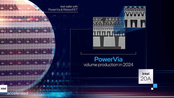
Intel 20A is a process rule that implements PowerVia, a new power distribution method for semiconductors called 'the industry's first backside power delivery', and RibbonFET, a 3D transistor technology, and is said to be adopted in products from the first half of 2024. I was. In addition, Intel 18A, which is an improved Intel 20A, is said to be adopted after 2025.
According to UDN, a Chinese economic media, Wang Rui, president and chairman of Intel China, Intel's Chinese subsidiary, said at an event that 'the development of the Intel 20A and Intel 18A manufacturing processes has been completed.' matter. This 'development completion' does not mean that Intel 20A and Intel 18A can be put into practical use immediately, but that Intel has decided all the specifications and requirements of Intel 20A and Intel 18A, performance targets, materials to be used, etc. I mean
In addition, Intel 18A, an improved version of Intel 20A, was to be adopted from 2025 onwards in the roadmap announced in 2021, but with the successful completion of development, the adoption has been brought forward to the second half of 2024. reported.
According to UDN, Intel 18A was supposed to use the Twinscan EXE scanner with a numerical aperture of 0.55 developed by ASML, a photolithography equipment manufacturer, but since the adoption of Intel 18A was brought forward from 2025 to the latter half of 2024, I will use the Twinscan NXE scanner with a numerical aperture of 0.33 that I have used so far.
Intel expects Intel 18A to be the industry's most advanced process node when the Intel 18A class manufacturing technology is applied to mass production in the second half of 2024.
by Fritzchens Fritz
The 'A' of Intel 20A refers to Angstrom (10 -10 m), which is further below nm (nanometer), which is 10 -9 m, but this means that the transistor can be reduced to the atomic level. It seems that it is an expected brand image and does not mean that the width or spacing of the circuit is actually measured in angstroms.
Related Posts:


in Hardware, Posted by log1i_yk