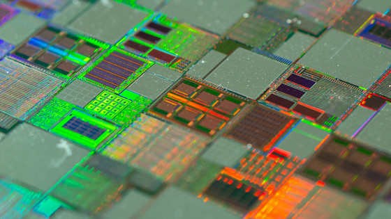
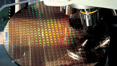
TSMC's next-generation 5nm process & 3nm process is scheduled to start mass production in 2022, and 2nm process is also under research and development
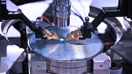
Q1 2021 Taiwan Semiconductor Manufacturing Co Ltd Earnings Call on April 15, 2021/6: 00AM --TSMC 1Q21 transcript.pdf
(PDF file) https://investor.tsmc.com/english/encrypt/files/encrypt_file/reports/2021-04/8b5438593d7b5d2181406a1b92d7304d6944c098/TSMC%201Q21%20transcript.pdf
TSMC Update: 2nm in Development, 3nm and 4nm on Track for 2022
https://www.anandtech.com/show/16639/tsmc-update-2nm-in-development-3nm-4nm-on-track-for-2022
◆ 5nm process 'N5'
In June 2020, TSMC began manufacturing semiconductors on the 5nm process 'N5' for the first time in the world. 'Already in the second year of mass production, the N5 has achieved better yields than originally planned,' said Wei. In 2021, N5 sales will reach 20% of TSMC's semiconductor manufacturing revenue. I'm expecting it, 'he said, emphasizing the success of N5 production.
According to technical media AnandTech , TSMC has not disclosed the uses of the semiconductors it produces. However, AnandTech claims that 'the N5 is known to be used in Apple's M1 and Apple A14 Bionic ,' claiming that the N5 is used in the SoC developed by Apple, TSMC's largest customer. ..
AMD has emerged as the second largest customer of TSMC, the world's largest semiconductor foundry, or that company is still number one-GIGAZINE

In addition, AnandTech said, 'We expect the demand for N5 to continue to grow in the next few years due to the increasing demand for
◆ Power-saving version 5nm process 'N5P'
Analysts at China Renaissance Securities , a Hong Kong-based financial firm, estimate that TSMC's N5 has approximately 170 million transistors per square millimeter. On the other hand, Samsung's 5nm process has about 125 to 130 million transistors per square mm, and Intel's 10nm process has about 100 million transistors per square mm. AnandTech rates TSMC's N5 as 'the densest technology available as of April 2021.'
Furthermore, according to AnandTech, TSMC plans to start manufacturing semiconductors using the power-saving 5nm process 'N5P' within a few weeks from the time of writing the article. TSMC says, 'N5P can increase operating frequency by up to 5% with the same power consumption as N5, and reduce power consumption by up to 10% at the same operating frequency.' 'Semiconductor design companies can smoothly transition from N5 to N5P. and can be carried out ', the characteristics of the N5P commentary has been.
◆ Performance-enhanced 5nm process 'N4'
TSMC will begin manufacturing semiconductors with the N4 in the second half of 2021 and plans to begin mass production in 2022.
The N4 adopts the same design rules and manufacturing equipment as the N5, but improves PPA (performance, power consumption, transistor density) compared to the N5, and expands the use of EUV lithography at the manufacturing stage compared to the N5. 'The N4 uses design rules that are compatible with the N5. We will leverage the strong technological foundation we have cultivated in the N5 to extend the 5nm process family,' said Wei.
What is the expected manufacturing technology 'EUV lithography' that can avoid the limits of 'Moore's Law'? --GIGAZINE
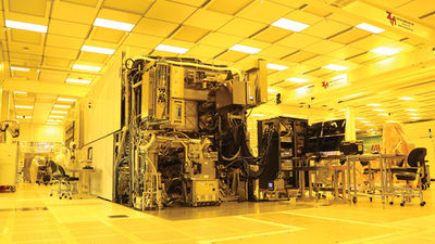
AnandTech said, 'By the time TSMC starts mass production of N4 in 2022, it will have three years of experience in EUV production and two years in N5 production. Therefore, the yield of N4 is high. , We can expect stable performance, 'he said, and he has high expectations for N4.
◆ 3nm process 'N3'
TSMC aims to start mass production of semiconductors using the 3nm process ' N3' in the second half of 2022.
Compared to N5, N3 is planned to improve performance by 10 to 15% with the same power and reduce power consumption by 25 to 30% with the same performance. In addition, N3 uses conventional technologies such as EUV lithography and DUV lithography, so there is no need to develop new technologies. AnandTech is 'Samsung is 3nm process' 3GAE for ', own the entire circumference gate FET (GAAFET) is' MBCFET are under development. 'This because there is no need the development of new technology in the N3 of TSMC against, We have the potential to significantly compete. '
'TSMC aims to start mass production of N3 in the second half of 2022. We are confident in both N5 and N3. Both will bring long-term benefits to TSMC. ', He says his expectations for N3.
◆ 2nm process
TSMC is conducting research and development on 2nm processes using GAAFETs.
In the 2020 (PDF link) annual report published by TSMC, 'Research and development of 2nm process is proceeding smoothly.' 'TMC has memory technology due to miniaturized process rules exceeding 2nm. We are conducting research and development focusing on fields such as 3D transistors and 3D transistors. '
AnandTech said, 'TSMC recently added $ 3 billion to its three-year R & D spend of $ 10 billion. TSMC is expanding its R & D. Is noteworthy. '
The following is a table summarizing each TSMC process node.
Process node | N7 | N7 | N7P | N7 + | N5 | N5P | N4 | N3 |
| Power consumption | 60% reduction | Up to 40% reduction | 10% reduction | 15% reduction | 30% reduction | 10% reduction | Reduction | 25-30% reduction |
| performance | 30% improvement | ?? | 7% improvement | 10% improvement | 15% improvement | 5% improvement | Improvement | 10-15% improvement |
| Silicon die area | 70% reduction | 37x reduction | --- | Approximately 17% reduction | 45% reduction | --- | --- | 42% reduction |
| Mass production start time | Q2 2019 | Second quarter of 2020 | 2021 | 2022 | Second half of 2022 |
Related Posts:
in Hardware, Posted by log1o_hf
