TSMC announces details of 5nm process/3nm process, 3nm process will start mass production in the second half of 2022
by Steve Jurvetson
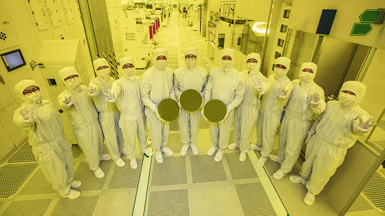
TSMC, a major semiconductor manufacturing foundry, explained the features of 5nm process and 3nm process at the regular technology symposium, and announced the roadmap and performance prediction.
'Better Yield on 5nm than 7nm': TSMC Update on Defect Rates for N5
https://www.anandtech.com/show/16028/better-yield-on-5nm-than-7nm-tsmc-update-on-defect-rates-for-n5
TSMC Details 3nm Process Technology: Full Node Scaling for 2H22 Volume Production
https://www.anandtech.com/show/16024/tsmc-details-3nm-process-technology-details-full-node-scaling-for-2h22
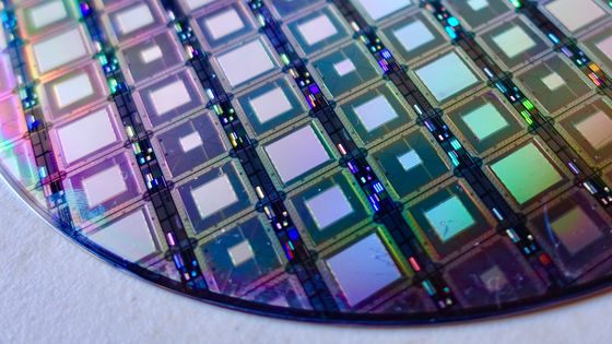
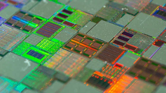
TSMC's 5nm process node ' N5 ' is a process node using extreme ultraviolet (EUV) photolithography . EUV photolithography is a circuit pattern generation technology that is also used in the 7nm process node “N7+” used in Huawei's 5G compatible SoC, Kirin 990.
According to TSMC, the N5 claims 1.8 times higher logic density, up to 15% better performance, and up to 30% less power than the 7nm process node “N7”. Furthermore, N5 can achieve a higher yield than N7.
According to TSMC, consumer products adopting N5 are planned to be produced in 2020, and technology news media AnandTech said, 'N5 may be adopted for the first time in Apple's next-generation SoC A14 chip series There is.' In fact, it is reported that production of the 5 nm process has started in June 2020.
The world's largest semiconductor manufacturing foundry ``TSMC'' officially starts manufacturing with 5 nm process-GIGAZINE

In addition, TSMC announced that it plans to launch a process node ' N5P ' in 2021 aiming at speed improvement of 5% and power reduction of 10% from N5. In addition, the same 5nm process node 'N4' was announced to enter risk production in the fourth quarter of 2021 and mass production in 2022, but did not announce performance.
And, the node 'N3' which adopted 3nm process of TSMC was announced. Performance of N3 is improved by 10 to 15% and power consumption is reduced by 25 to 30% compared to N5, so N3 will start risk production in 2021 and mass production is planned in the second half of 2022. I will. For the 3nm process, Samsung has announced its own process node, 3GAE , which AnandTech says 'in terms of power and performance, N3 and 3GAE are equivalent, but N3 is a significant leader in logic density.' I will.
The table below summarizes the comparison of each TSMC node.
Process node (Compare in parentheses) | N7 (16FF+) | N7 (N10) | N7P (N7) | N7+ (N7) | N5 (N7) | N5P (N5) | N3 (N5) |
| Power consumption | 60% reduction | Up to 40% reduction | 10% reduction | 15% reduction | 30% reduction | 10% reduction | 25-30% reduction |
| performance | 30% improvement | ? | 7% improvement | 10% improvement | 15% improvement | 5% improvement | 10-15% improvement |
| Silicon die area | 70% reduction | 37 times reduction | - | About 17% reduction | 45% reduction (Logic density 1.8 times) | - | 42% reduction (Logic density 1.7 times) |
| Mass production start time | Q2 2019 | Q2 2020 | 2021 | Second half of 2022 |
Related Posts:


in Hardware, Posted by log1i_yk