Why it costs trillions of dollars to build a modern semiconductor fab
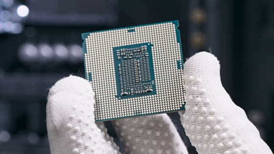
Semiconductors are materials that can change their electrical conductivity by orders of magnitude, blocking or allowing the flow of electrons, and are necessary to create all kinds of electronic devices, including PCs. While the cost and size of semiconductors have decreased over decades of technological development, the cost of semiconductor manufacturing plants has skyrocketed to trillions of yen.
How to Build a $20 Billion Semiconductor Fab
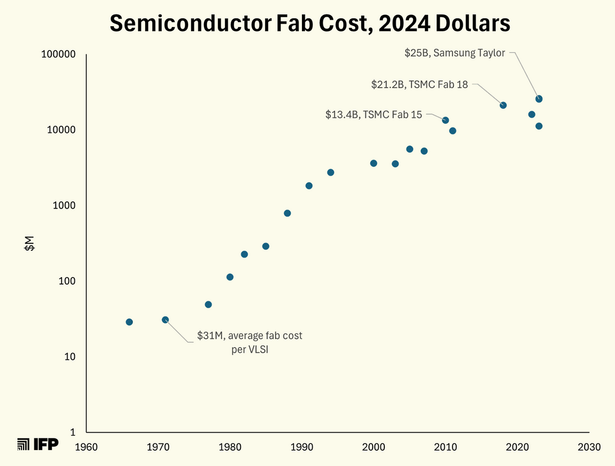
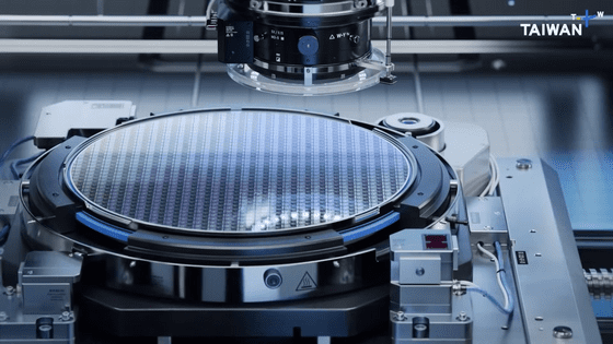
The average construction cost of a semiconductor factory was $31 million (about 4.8 billion yen) in the 1970s, but by 2020, factories costing $20 billion (about 3 trillion yen) were being built one after another.
By
The reason for this improvement in construction costs is the semiconductor manufacturing process. A cross-section of a computer chip is shown below, with many layers of layers.
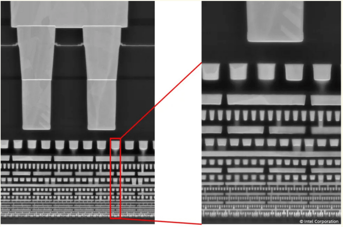
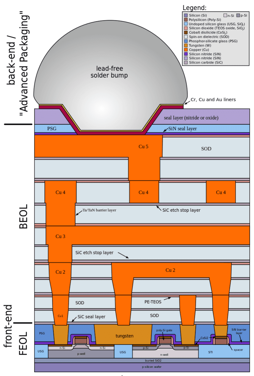
The diagram below shows the structure of a CMOS chip from the early 2000s. The main semiconductor parts such as transistors are installed in the area marked 'FEOL' at the bottom of the chip, and many parts are interconnected in the BEOL layer above. As the number of transistors used increases, the wiring becomes more complex, and it is not uncommon to have more than 10 BEOL layers for wiring.
By
Chips are built up by stacking these complex structures layer by layer.
By Fabrication Engineering at the Micro- and Nanoscale
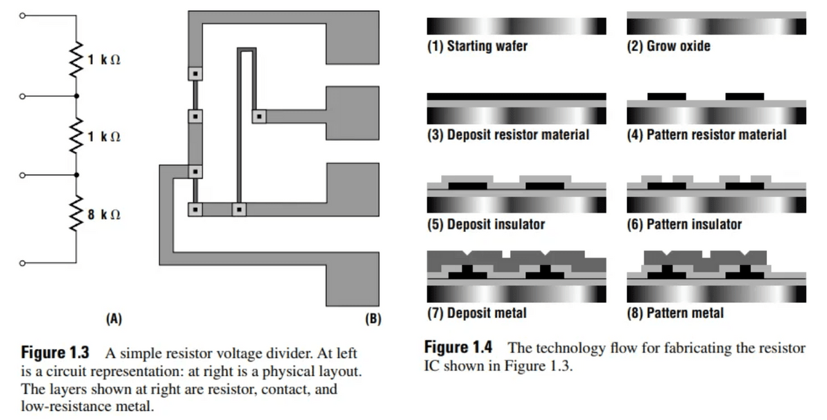
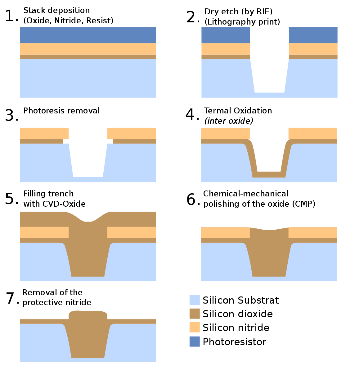
The construction of a chip structure involves four operations: layering, patterning, doping, and heat treatment.
・Layering
Layers just one nanometre thick – one hundred thousandth the thickness of a human hair – are added to the surface of the wafer. As technology advances, the deposition requires greater precision, and modern atomic layer deposition techniques are now capable of creating single atomic layers.
・Patterning
A specific pattern is inscribed onto the wafer, then material is selectively removed as required - a modern technique used is photolithography, where a coating of light-sensitive material is applied and then light is shone through a mask plate containing the inscribed pattern, causing a chemical reaction that 'prints' the pattern.
·doping
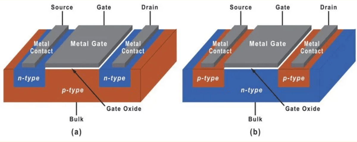
By introducing very small amounts of impurities into semiconductor materials, their electrical conductivity is altered. Different impurities produce n-type semiconductors with an excess of free electrons and p-type semiconductors with an excess of holes , and by arranging n-type and p-type semiconductors in the right order, a transistor can be created.
By
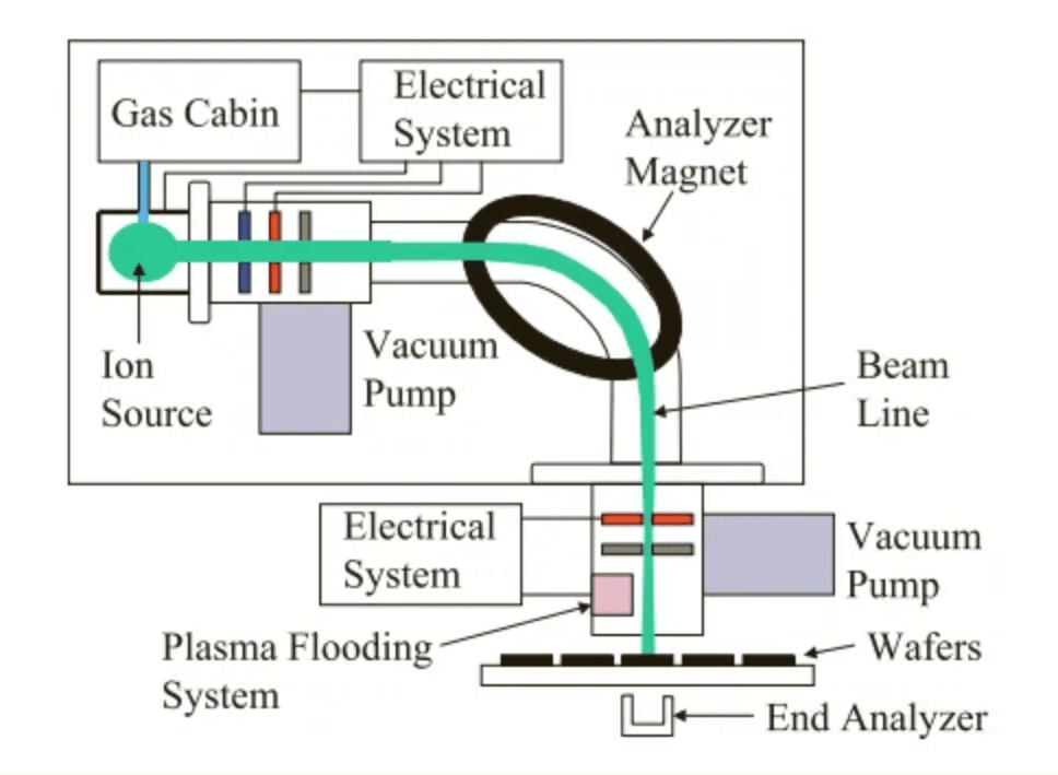
In the past, doping was done by reacting gasified atoms with the wafer, but nowadays, doping is done by irradiating it with an ion beam.
By Xiao 2012
·Heat treatment
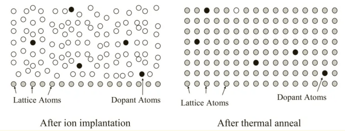
Ion beam irradiation damages the silicon's crystal structure, so the crystal structure is repaired by a heat treatment that involves heating the wafer to 1,000 degrees for a few seconds and then slowly cooling it.
By Xiao 2012
In addition to the four basic processes, semiconductor manufacturing has many sub-processes. One of the sub-processes is 'polishing.' Semiconductors are built in many layers, so there is a large variation in thickness with each additional layer. To make the surface smooth, chemical mechanical polishing (CMP) is used to polish the wafer.
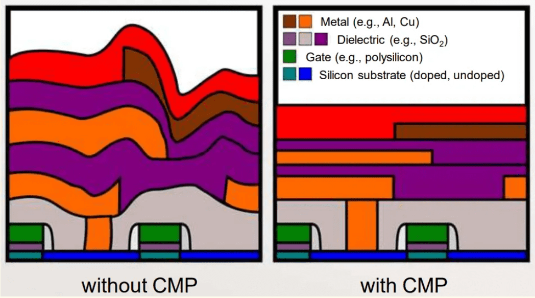
By
CMP is also used to fill holes created by etching.
By
'Cleaning' is another important support process. Even the smallest airborne particles can cause semiconductors to malfunction, so the wafers must be constantly cleaned with solvents and pure water. Many parts of the process are also carried out in clean rooms where airborne particles are reduced to an absolute minimum, and the wafers are measured at various points in the process to determine if there are any mistakes or defects.
By Xiao 2012
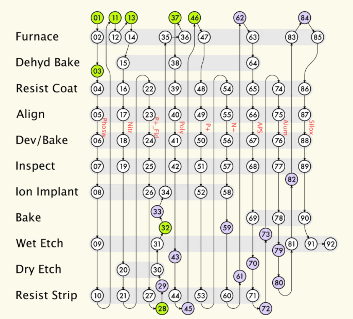
Semiconductor structures are slowly built up through the repeated application of four main processes and numerous sub-processes. Modern manufacturing requires more than 80 masks and thousands of process steps.
By
Once the circuit structure is complete, it moves to assembly and packaging, where the wafer is separated into individual chips, each of which is connected to wires and then given a protective coating.
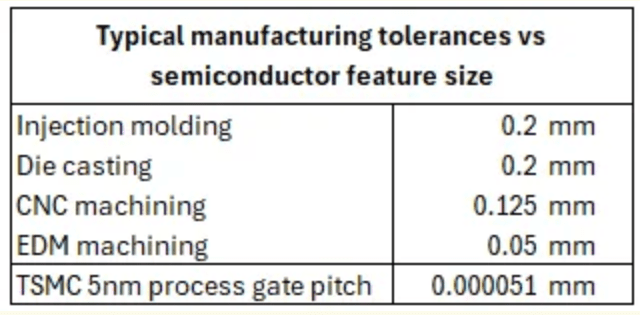
Not only are semiconductors complex products with many process steps, but they are also incredibly small, requiring extreme precision. While typical manufacturing processes can tolerate errors of 0.05mm to 0.2mm, semiconductors have process gates that are only 0.000051mm (51nm) apart. And even a single particle can cause a short circuit, rendering the entire chip non-functional.
The history of semiconductor manufacturing is a record of fighting against tiny elements with destructive effects. In the 1940s, when semiconductors were being researched at Bell Labs, a mysterious component failure occurred. The cause was a tiny copper atom that had adhered to the researcher's hand when he touched a copper doorknob. Early semiconductor manufacturers also realized that semiconductor yields were affected by the phases of the moon, employees' bathroom timing, and female employees' menstrual cycles.
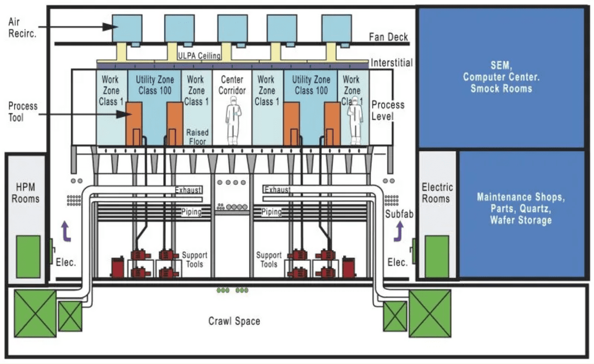
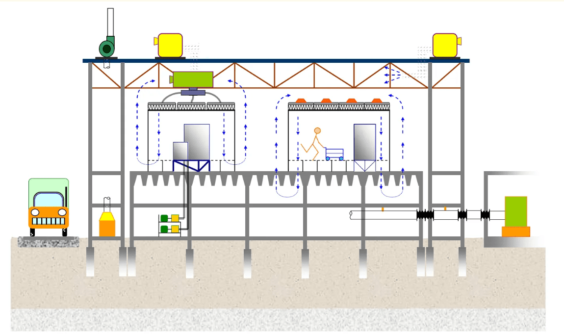
As semiconductor technology has evolved, the level of cleanliness required during manufacturing has also increased. Modern semiconductor factories have four levels to create a clean environment. The top level contains fans and filters that support air circulation for the clean room on the second level. Below the clean room are two support levels that contain piping, wiring, and equipment for the clean room facilities.
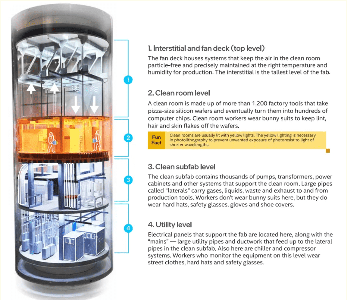
By Intel
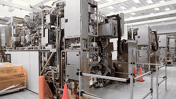
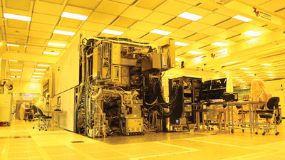
The cleanroom will house a variety of semiconductor manufacturing equipment, including lithography tools, chemical vapor deposition tools, ion implantation tools, and wet benches for cleaning and etching. The tools are grouped together by type to isolate the chemicals used in each process. To minimize the impact of columns and walls, the roof is made of a large, long truss structure to keep the cleanroom space as open as possible.
By
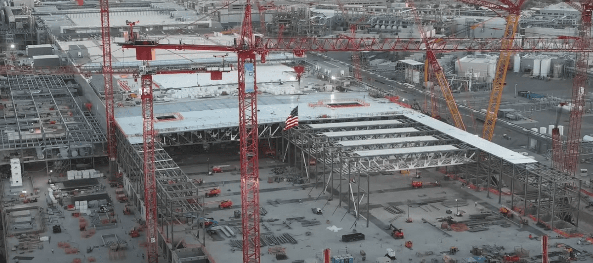
If you look at Intel's semiconductor factory under construction, you can see the huge truss structure for the clean rooms.
By
In a typical home, there are about 500,000 particles of 0.5 μm or more per cubic foot of air, and about 100,000 particles floating in an operating room, but in semiconductor factory clean rooms, the number of particles of 0.5 μm or more per cubic foot of air is controlled to 10 to 100 or less depending on the class. To prevent particles from entering, clean rooms are kept at positive pressure relative to the outside, and the air is replaced 5 to 10 times per hour.
By
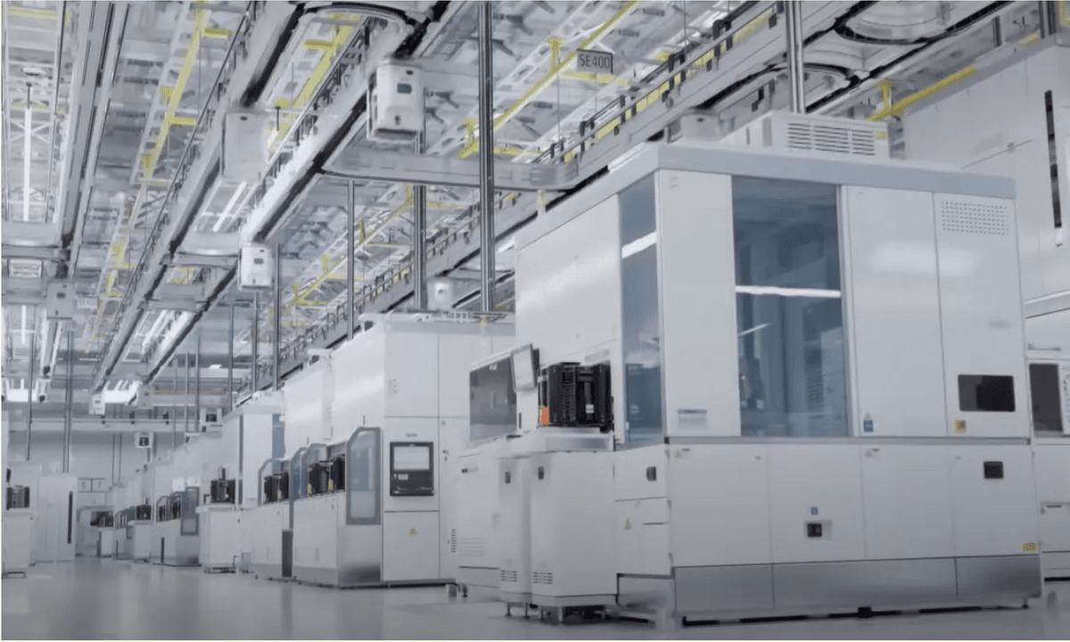
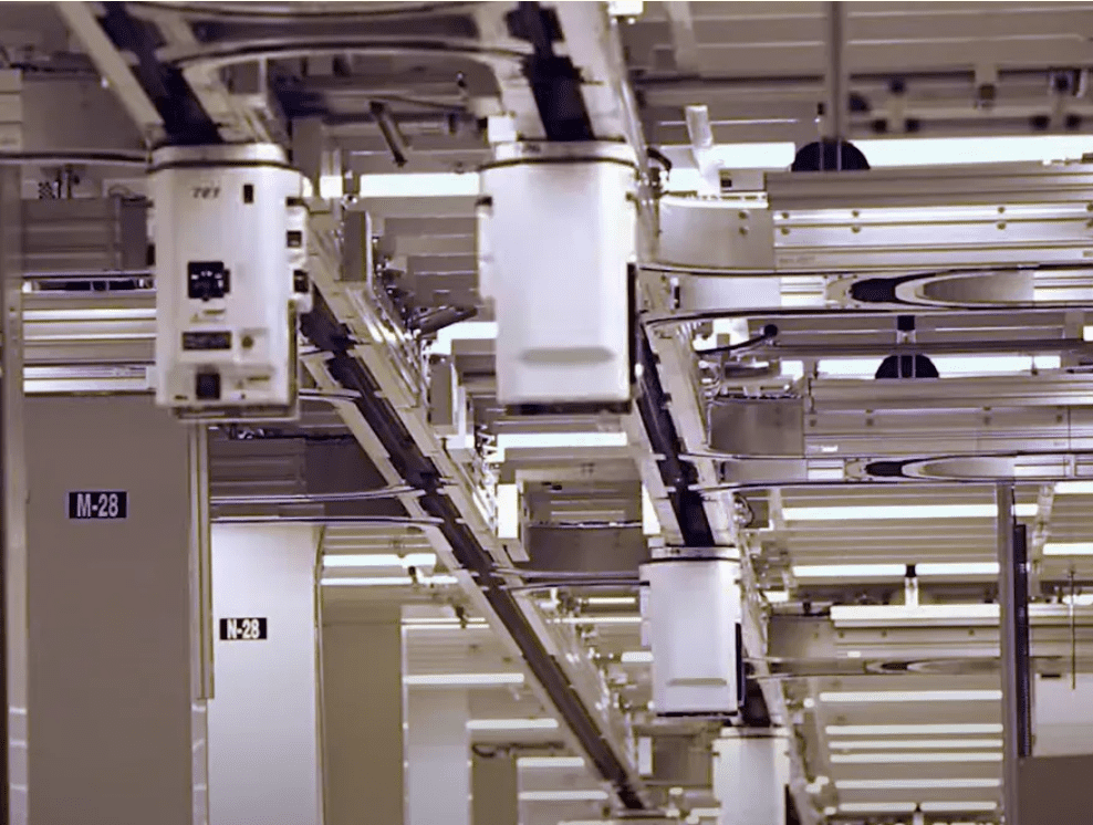
Because the air that comes into direct contact with the wafers must be even cleaner, with no more than 0.1 particles of 0.5 μm or larger per cubic foot, manufacturers create mini-cleanrooms within cleanrooms in which to process the wafers. Sealed pods called FOUPs are used for transport between equipment.
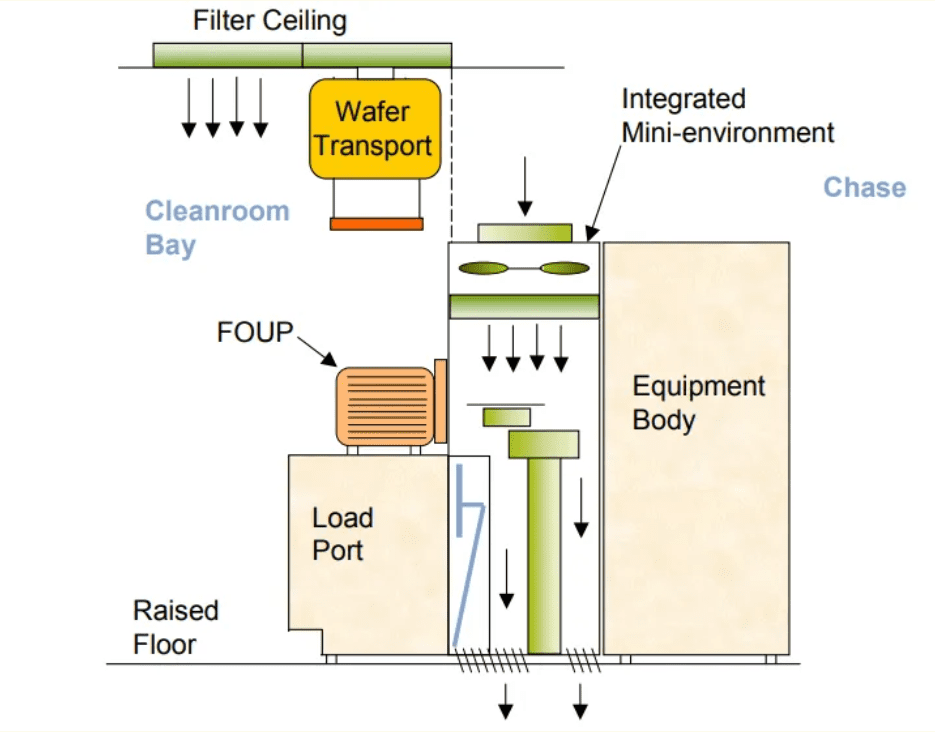
In modern factories, FOUPs consist of a rail system mounted on the ceiling. Due to the large number of manufacturing processes, the wafers can travel through the factory over a period of months, and there can be tens of thousands of wafers in the factory at any one time. To handle such a large number of wafers, the transport system must be able to handle the traffic smoothly, with many kilometers of track and thousands of transport vehicles.
By Intel
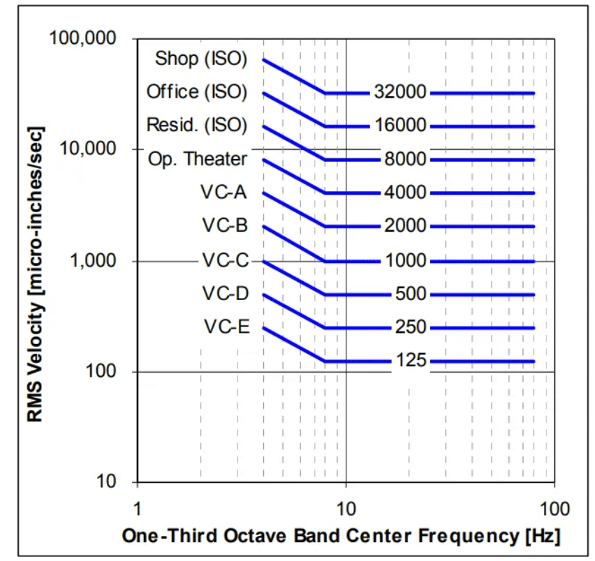
It is not just airborne particles that affect the manufacturing process. Semiconductor factories are also very sensitive to vibrations, and in the past there have been cases where an exhaust vent 100m away from the factory caused unacceptable vibrations on the cleanroom floor. The factory must absorb 100 times more mechanical energy and 50 times more airflow than a traditional building, and keep vibrations several orders of magnitude below the threshold of human perception. The figure below shows the vibration requirements for various buildings, and semiconductor factories are built according to VC-D or VC-E.
By
To minimise vibration, cleanroom floors are constructed of concrete waffle slabs roughly one metre deep, supported by closely spaced columns to make them as stiff as possible. A metal floor sits above the slab, isolating the manufacturing machinery from the floor where people walk. Equipment with particularly stringent requirements, such as lithography equipment, requires measures such as active vibration dampers to sense and cancel vibrations.
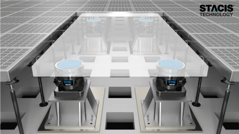
By
In some cases, the cleanroom floor may be physically separated from the floors of the rest of the building.
By
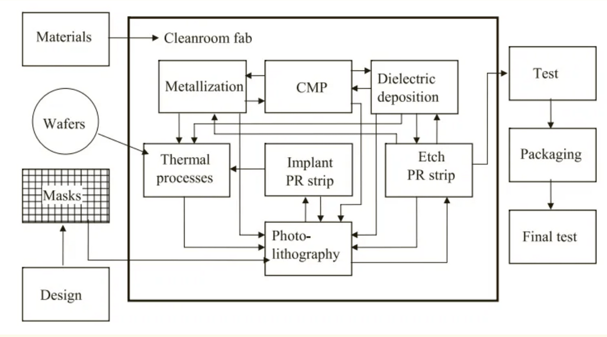
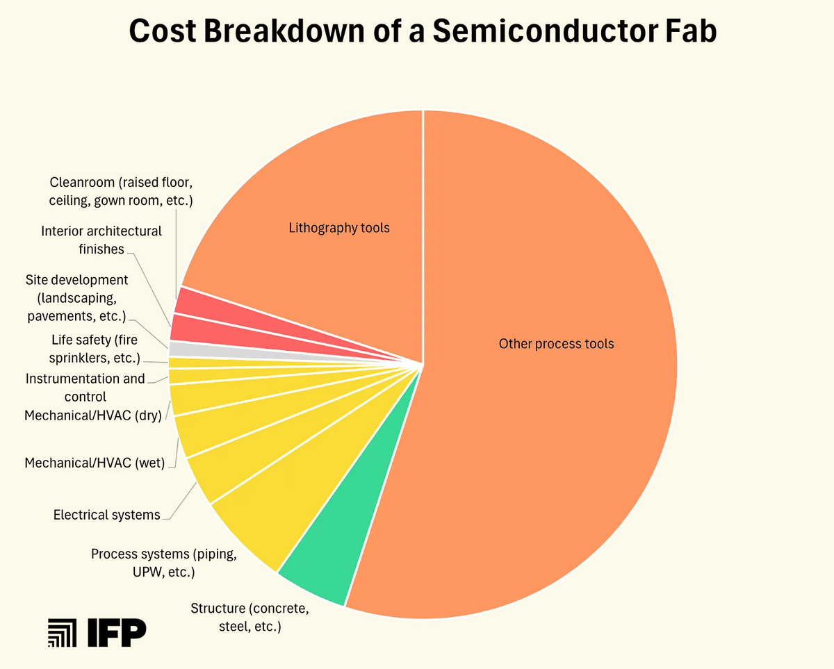
Bayat et al. 2012When you consider not only the construction of clean rooms, but also the pipes connected to the manufacturing equipment and the storage of chemicals, it is not surprising that the construction of a semiconductor factory requires a vast site, a large amount of materials, and special construction methods, making it very expensive. However, in modern semiconductor factories, the cost of the manufacturing equipment used inside is higher than the cost of building the factory. In the 1980s, the construction cost and the cost of the manufacturing equipment were about half and half, but by the late 1990s the cost of the manufacturing equipment had already come to account for the majority of the costs.
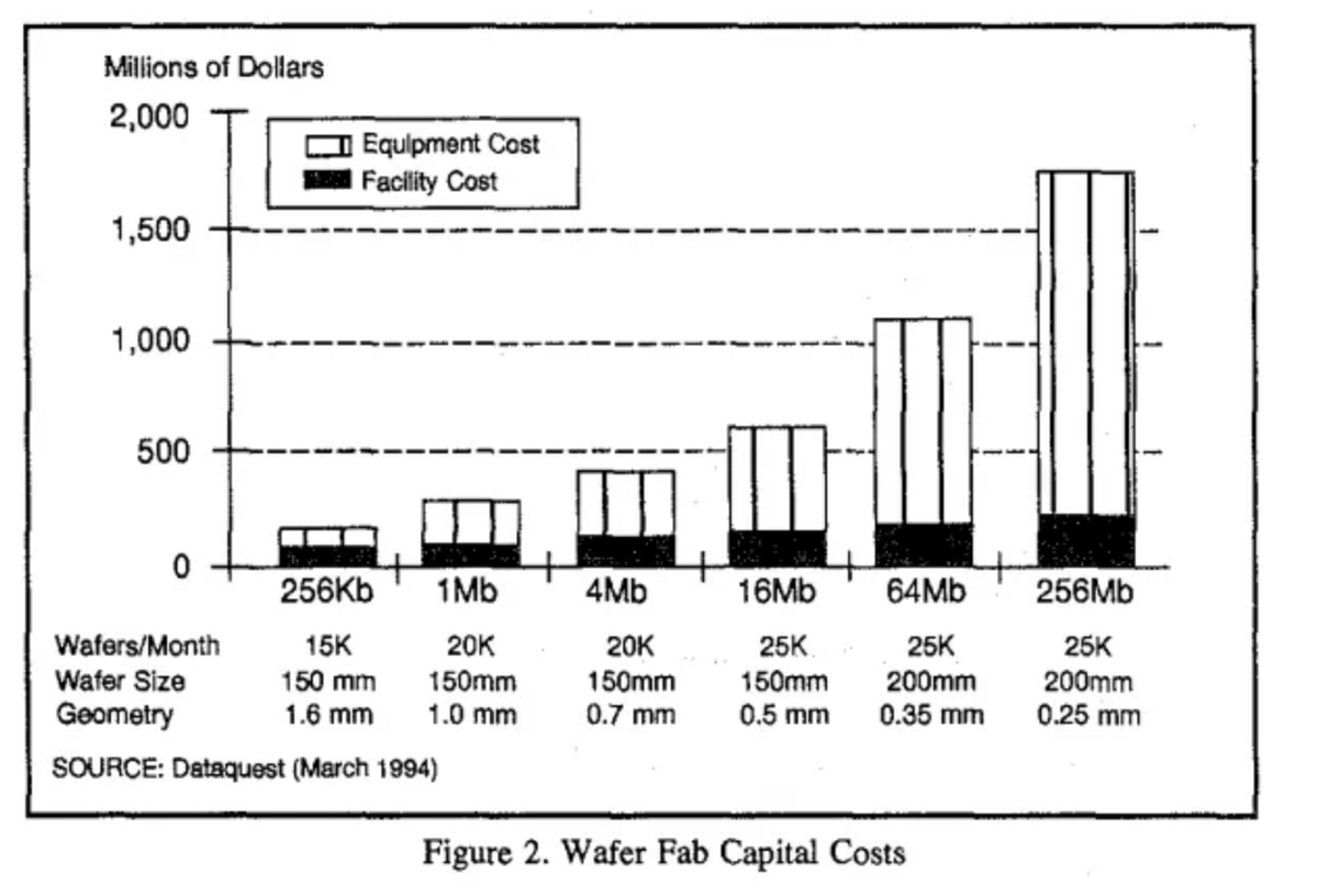
By
Among all manufacturing equipment, the cost of lithography equipment is particularly high, and in some cases the cost of lithography equipment alone can be as high as the construction cost of a factory. Following lithography equipment, the cost of deposition, cleaning, and etching equipment is also high.
By
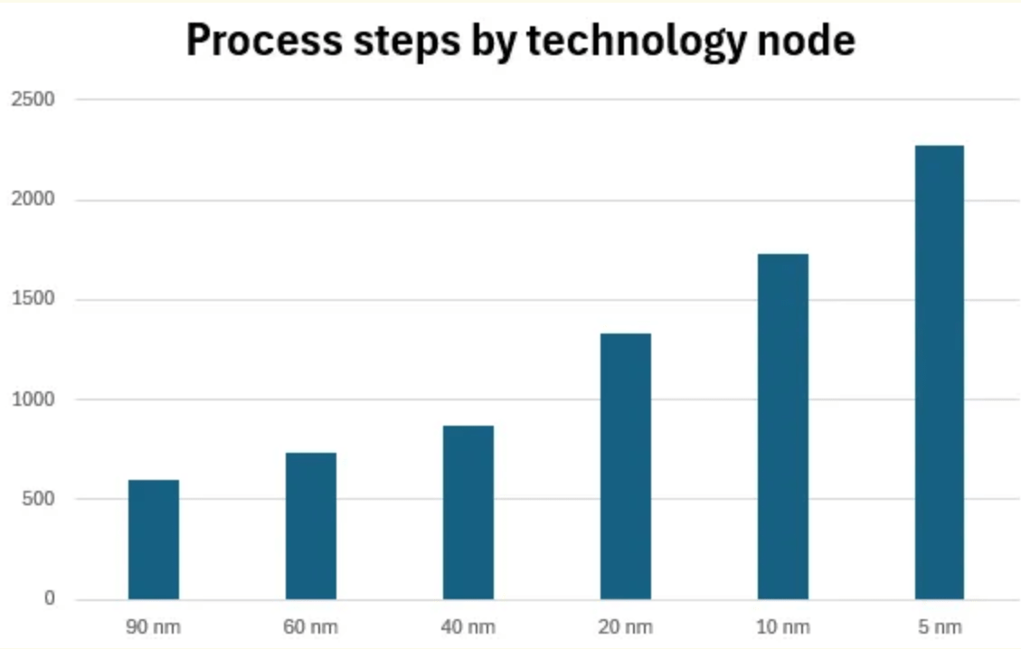
As semiconductor manufacturing technology improves and transistors get smaller, the costs of semiconductor foundries are rising. Each more advanced process node requires more expensive manufacturing equipment and more layers and steps, increasing manufacturing costs by 30%.
By Practices of Wafer Fab Operations
Rising factory costs have also caused the semiconductor industry to restructure. When factories were cheap, every chipmaker could afford to build its own factory, but as manufacturing costs have risen, fewer manufacturers have the production capacity to cover those costs. For example, a 150mm wafer manufacturing factory can run 10,000 wafers per month to be efficient, but a factory making 300mm logic wafers needs to run 40,000 wafers per month to be at peak efficiency.
As a result, only a few companies, such as TSMC, Samsung, and Intel, manufacture cutting-edge semiconductors, while companies such as Apple and NVIDIA design chips and have them manufactured by 'foundries' such as TSMC, which own semiconductor manufacturing plants. The foundries can achieve the scale required to efficiently operate cutting-edge factories by accepting orders from a variety of chip companies.
As a result, semiconductor factories have become enormous in size, and the cost of building them has become enormous due to the need to perform atomic-level operations 24 hours a day, 365 days a year within these huge factories.
Related Posts:

in Free Member, Hardware, Posted by log1d_ts