The possibility that 'metal - air transistor' that breaks the limit of Moore's law replace semiconductor
Instead of semiconductors whose limits of " Moore's Law " are whispering, new technology called " Metal-Air Transistor " is being developed. It is said that Moore's Law will be maintained for another 20 years by realizing a metal-air transistor.
Metal-Air Transistors: Semiconductor-Free Field-Emission Air-Channel Nanoelectronics - Nano Letters (ACS Publications)
https://pubs.acs.org/doi/10.1021/acs.nanolett.8b02849
New Metal-Air Transistor Replaces Semiconductors - IEEE Spectrum
https://spectrum.ieee.org/nanoclast/semiconductors/devices/new-metalair-transistor-replaces-semiconductors
The empirical rule of "Intel's founder Gordon Moore," the number of transistors in a semiconductor integrated circuit doubles every 18 months (every 2 years later) "is a development goal for the semiconductor industry as a whole Miniaturization technology has been developed on the street and the performance of semiconductors has improved. However, as the line width approaches the atomic level, it is difficult to maintain Moore's limit, and Moore's Law reaches the physical limit at the latest in 2025 and becomes impossible to realize at the latest.
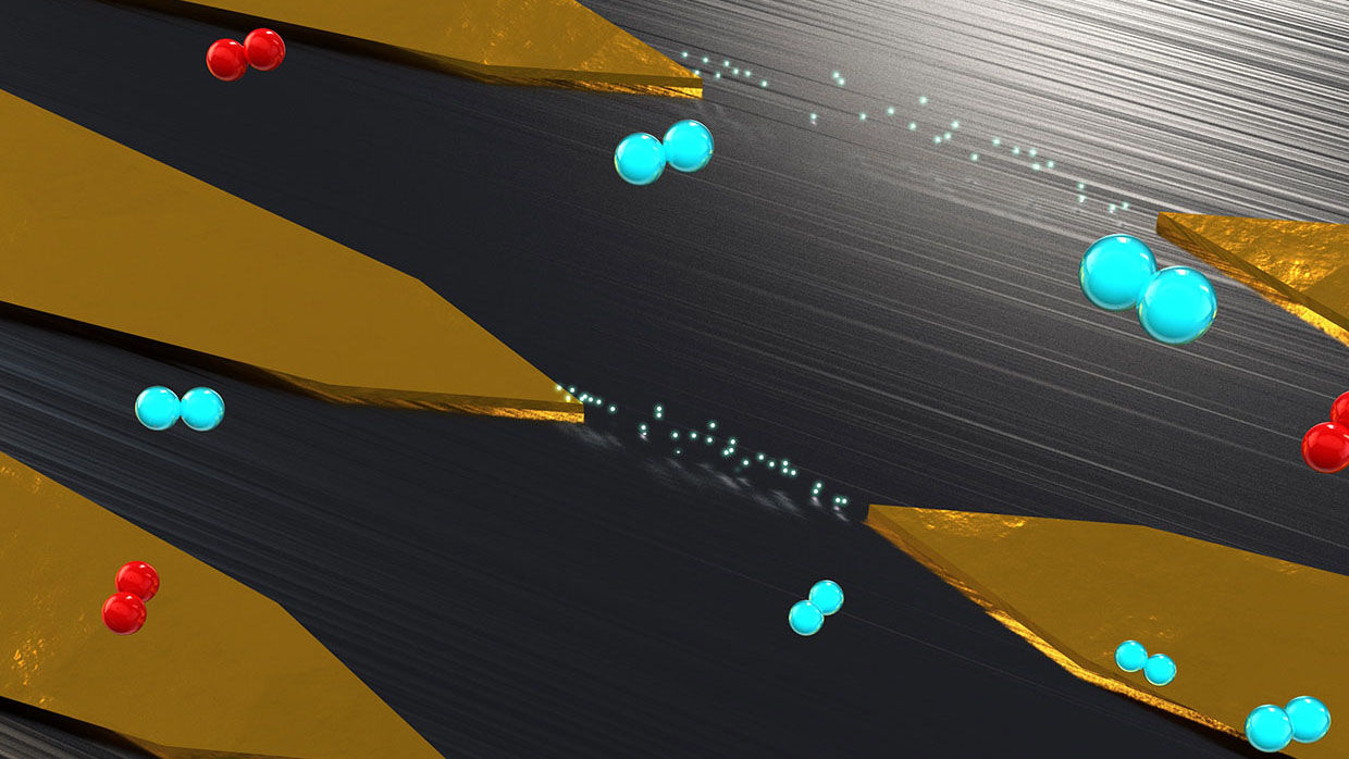
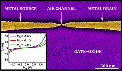
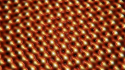
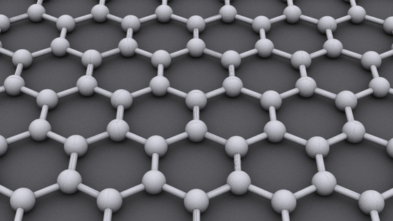
Meanwhile, researchers at RMIT University in Australia developed a metal-based air channel transistor (ACT). Unlike charge-based semiconductors, ACT is a technology to construct a transistor network vertically from a substrate by using a face-to-face metal gate of each of the source and drain separated by an air gap (air layer) of less than 35 nanometers And that. Since the air gap is smaller than the mean free path of electrons in the air, electrons can move in air at room temperature without splashing.
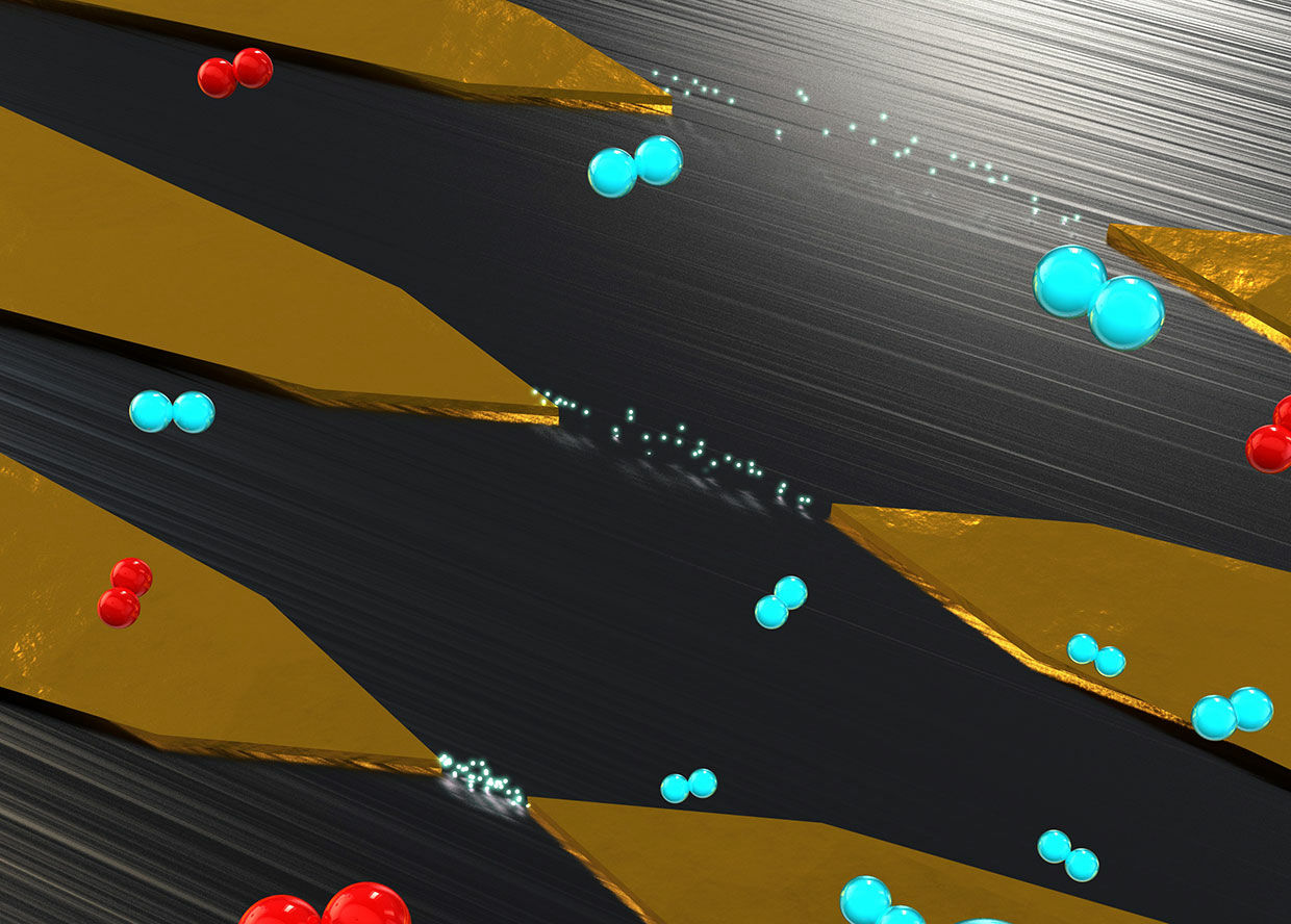
By stopping the pursuit of miniaturization and focusing on the three-dimensional structure, ACT can increase the number of transistors per unit area. Dr. Schulti Nilanta, who is developing ACT, said, "Unlike traditional silicon-bound transistors, the devices we develop are approaches that can be manufactured from the board in a bottom-to-top fashion, making an optimal air gap We can build a complete 3D transistor network if we can, "he says.
The use of metal and air rather than semiconductors as the main material of the transistor is to be able to spread the emitter and collector in one process, the existing silicon manufacturing process can be diverted to manufacture ACT, doping · heat treatment · Dr. Nilanta emphasizes that there is a great merit in terms of significantly reducing the processing steps compared to semiconductors, as it is unnecessary to perform an essential treatment such as oxidation on silicon semiconductors, which greatly reduces manufacturing costs.
Moreover, by replacing silicon with metal, there is a possibility that ACT can be made on any dielectric surface, it is flexible and can be worn on the body by building a device in ultra-thin glass or plastic It is expected to be applicable as well.
As ACT finished the proof of concept, researchers said that in the future we will go to the step of testing various source + drain configurations. Lithography, deposition technology and selection of the metal to be used will be carried out in order to raise the safety by using more durable materials and improve the efficiency of the components. The theoretical speed of ACT is in the region of THz (terahertz) which is about 10,000 times the speed at which the current semiconductor device operates, and we will develop a commercial level electrolytic emission air channel transistor over the next ten years It seems that we are depicting a roadmap that is comparatively easy to do.
Related Posts:

in Hardware, Posted by darkhorse_log