Pointed out that 'motherboard' is hindering the development of hardware, what is the next generation technology to replace motherboard?
By
IEEE Spectrum, a news site related to hardware engineering run by IEEE, a professional organization such as electrical engineering, titled “Goodbye, Motherboard”, “ A printed circuit board like a motherboard hinders hardware development. ” Insist.
Goodbye Motherboard Hello Siliconinterconnect Fabric-IEEE Spectrum
https://spectrum.ieee.org/computing/hardware/goodbye-motherboard-hello-siliconinterconnect-fabric
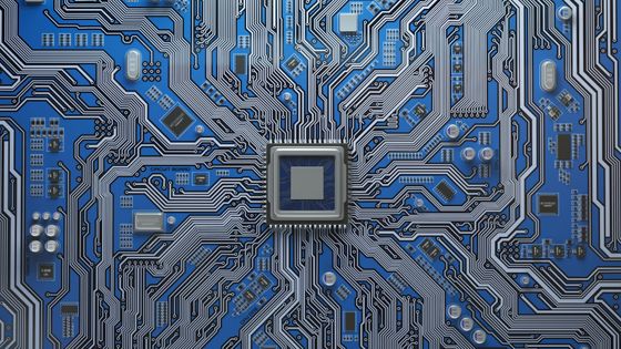
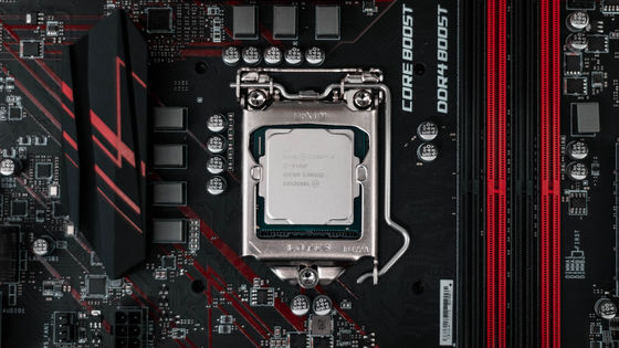
Devices such as smartphones and notebook PCs are required to be as small as possible. However, the problem is in the “printed circuit board”. Looking at the SoC , which is the core component of smartphones, the chip, which is an essential part of its function, is only one-twentieth the size of the SoC itself. It is the printed circuit board that bothers to pack the chip into a 20x larger package.
By
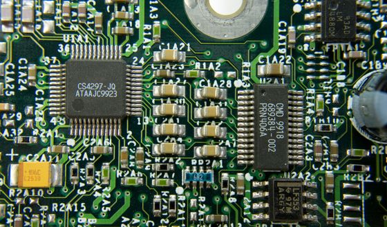
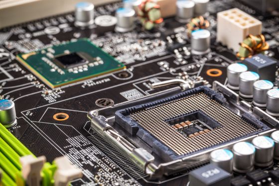
Because of the structure of printed circuit boards, warping is inevitably produced. When trying to solder-bump a chip, it is difficult to bring the chip and printed circuit board close to the distance required for power supply and signal transmission / reception due to the warping of the printed circuit board. Therefore, it is necessary to package silicon chips and form solder bumps on the printed circuit board as an integrated circuit .
The impact of chip and package size differences is enormous. Of course, the larger package means that it is difficult to save space, which is contrary to the purpose of devices where “smallness” is important, such as smartphones and smart watches. In addition, as is done on most printed circuit boards, when intercommunication is performed between chips, the processing speed decreases as the distance between chips increases.
By
In addition to this size problem, there is also a problem that heat dissipation efficiency deteriorates once packaged. This heat dissipation problem has been a serious hardware problem for decades.
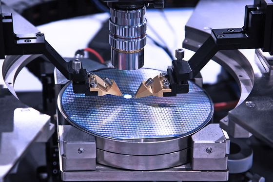
The “ Silicon-interconnect fabric (Si-IF) ” that directly connects the chip to the wiring on the silicon piece solves these problems. When the printed circuit board and IC and other packages are abolished, and chips, processors, memory dies, RF chiplets, VRMs , inductors, capacitors, etc. are bonded to relatively thick silicon from 500 µm to 1 mm, by connecting the wiring in layers, Compared to printed circuit boards, the distance between each chip can be reduced from 500µm to 2µm. In addition, the distance between the chip and the I / O port can be reduced from 500μm to 10μm, which can save a lot of space. This space saving improves processor performance by reducing the distance between chips. In addition, since silicon is a material with excellent thermal conductivity, it is possible to increase heat dissipation by as much as 70% by attaching a heat sink on the silicon substrate.

On the other hand, the disadvantage of silicon is its price. The IEEE states that silicon is 10 times more expensive per unit area than
The design and prototyping of this Si-IF is currently underway, and a joint research group at the University of California at Los Angeles and the University of Illinois at Urbana-Champaign has created a 40-chip Si-IF GPU on a trial basis. thing. It seems that this GPU has succeeded in reducing energy consumption by 80% while achieving 5 times the calculation speed compared to a GPU with 40 chips on a conventional printed circuit board.
The benefits of Si-IF also exist in manufacturing. SoC has the feature that the yield decreases exponentially as the area increases, and it is difficult to design, so the manufacturing cost is high. On the other hand, Si-IF is designed to connect the chip directly to the silicon substrate, so the design is inexpensive. Furthermore, the silicon substrate has a very simple structure, so the yield is almost 100%.
By ssp48
In order to put this Si-IF into practical use, some problems still remain. The first is to establish and demonstrate a Si-IF manufacturing process that can be used on a commercial level. The second is to design a new heat sink that takes advantage of the superior thermal conductivity of silicon. The third is to design a chassis mount connector cable specialized for silicon. Fourth, Si-IF has a characteristic of directly bonding the chip to silicon, so it is difficult to replace the chip, so it is necessary to ensure redundancy.
There are other problems, but a project called Common Heterogeneous Integration and IP Reuse Strategies (CHIPS) by the US Defense Advanced Research Projects Agency (DARPA) is already working on solving some problems.
Related Posts:


in Hardware, Posted by darkhorse_log