Development of the NAND flash memory used in SSDs is currently underway with the goal of increasing the number of layers to 1,000. What challenges must be overcome to increase capacity?
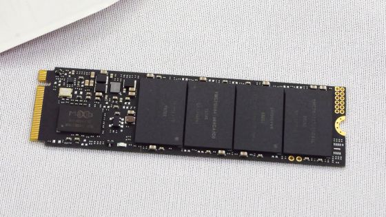
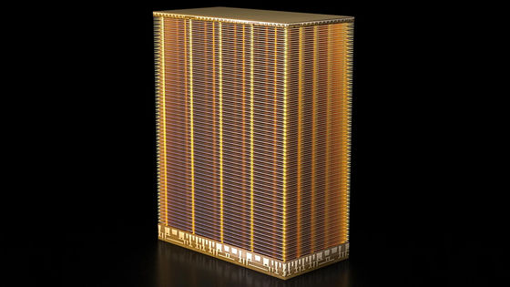
NAND flash memory, which is installed in data storage media such as SSDs, adopts an approach of 'vertically stacking memory cells' to increase the storage capacity per chip. In November 2024, SK hynix announced a 321-layer NAND flash memory , but memory manufacturers are already developing it with the aim of achieving more than 1,000 layers within a few years.
NAND Flash Targets 1,000 Layers
https://semiengineering.com/nand-flash-targets-1000-layers/
In addition to stacking memory cells vertically, there is also a method of writing two or more bits of data to one memory cell to increase the capacity of NAND flash memory. QLC NAND, which can write four bits of data to one memory cell, is already available on the market, and research is also underway on PLC NAND, which can write five bits of data. However, the method of writing multiple bits of data to one memory cell has the disadvantage of slower write speed.
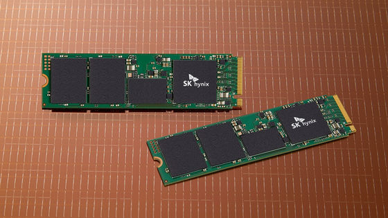
The technique of 'vertically stacking memory cells' has attracted attention as a way to increase storage capacity while maintaining data transfer speed, and memory manufacturers are competing to improve stacking technology. In November 2024, South Korea's SK hynix announced a 321-layer NAND flash memory, which it said could achieve larger capacity and faster data transfer than 238-layer NAND flash memory.
SK hynix begins mass production of the world's first 321-layer NAND flash memory, improving data transfer speed by 12%, read performance by 13%, and power efficiency by more than 10% from existing 238-layer NAND - GIGAZINE
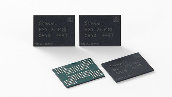
According to Mohan Bahrn, general manager of semiconductor company ACM Research, memory manufacturers are working on research and development with the aim of stacking more than 1,000 layers. However, to achieve more than 1,000 layers, several challenges must be overcome.
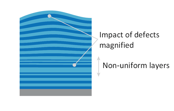
One of the challenges is that 'when memory cells are stacked in large numbers, even a small difference in thickness can make a big difference.' To solve this problem, ACM Research is studying a technique to 'periodically rotate the wafer 180 degrees during memory cell wafer manufacturing.' According to Byrne, by periodically rotating the wafer, it is possible to keep the misalignment within 1%.
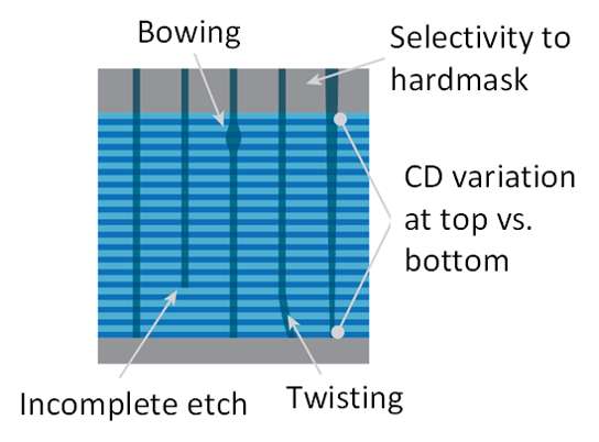
In addition, when stacking memory cells, it is necessary to form memory through-holes that penetrate the stacked memory cells, but the more layers there are, the more difficult it becomes to form the memory through-holes. Each manufacturer is also working on developing new materials to replace existing materials in order to realize precise and durable memory through-holes.
Furthermore, there are geopolitical issues with the realization of NAND flash memory with more than 1,000 layers. The United States restricts exports of NAND flash memory with more than 128 layers to China, so Chinese companies such as YMTC have to adopt a method of 'connecting multiple memory stacks of up to 128 layers'.
In addition, technology media Semiconductor Engineering says that 'it will take several years to solve various problems and realize NAND flash memory with more than 1,000 layers.'
Related Posts:
in Hardware, Posted by log1o_hf

