Micron announces 232-layer 3D NAND flash memory, data transfer speed increased by 50% to reach 2.4 Gbit / s
First to Market, Second to None: the World's First 232-Layer NAND
https://www.micron.com/about/blog/2022/july/first-to-market-second-to-none-the-worlds-first-232-layer-nand
Micron Is First to Deliver 3D Flash Chips With More Than 200 Layers --IEEE Spectrum
https://spectrum.ieee.org/micron-is-first-to-deliver-3d-flash-chips-with-more-than-200-layers
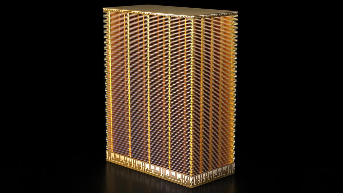
'3D NAND flash memory' is a three-dimensional stack of conventional NAND flash memories that stacks memory cell arrays in the vertical direction to increase memory capacity, improve write speed, and save power. is. In the development of this 3D NAND flash memory, four camps, Samsung in South Korea, SK Hynix in South Korea, Intel & Micron, Kioxia & Western Digital, are competing, but Micron has newly released 232-layer 3D NAND flash memory. Announced. This is the first time that 3D NAND flash memory has exceeded 200 layers, and so far 176 layers of 3D NAND flash memory has been the largest.
According to Micron, the company's first 232-layer 3D NAND flash memory doubles the density of bits stored per unit area compared to competing memory, reaching 14.6 Gbit of storage capacity per square millimeter. increase. The chips that make up this 3D NAND flash memory have a size that slightly exceeds 1 cm on each side, yet the capacity has been successfully increased by concentrating 232 layers.
The next generation of #NAND technology is here — 232 layers of it. Introducing our newest and coolest storage innovation yet!
— Micron Technology (@MicronTech) July 26, 2022
More layers, maximum performance. Learn more about what the future has in store: https://t.co/TmU5l298gt # 232NAND pic.twitter.com/XzVpHWc5qf
According to a survey by the International Data Corp (IDC), 81 trillion gigabytes (81ZB: zettabytes) of data were generated in the year 2021, and the amount of data generated in the year will increase to 221ZB in 2026. It is speculated that. Under these circumstances, Alvaro Trade, vice president of data center storage at Micron, said, 'Storage needs to innovate to keep up with the sheer volume of data generated each year.' I am.
The 232-layer 3D NAND flash memory is a combination and expansion of technologies that Micron has developed so far. In the first place, 3D NAND flash memory is built on the bottom layer of CMOS logic and other circuits, designed to control read and write operations and move data to and from the chip as quickly and efficiently as possible. .. By optimizing the movement of bus data and improving the connection between layers such as reducing the capacitance during input and output of the chip, the data transfer speed of Micron's 3D NAND flash memory has been improved by about 50%, 2.4 Gbit. It is reported that / s has been reached.
In 3D NAND flash memory, layers of conductor and insulator are alternately arranged and etched to form deep and narrow holes, and these holes are filled with material. An important limitation of technology is the technology that reliably fills the holes in all these layers. In Micron's process, instead of etching 232 layers at once, they divide them into two parts, perform everything from etching to refilling holes, and then stack the two components. 'This is an amazing engineering feat and one of the biggest challenges we have succeeded in overcoming,' said Trade.
In addition, each memory maker is trying to increase the bit density of flash memory by loading more layers or storing multiple bits in one memory cell. The 232-layer 3D NAND flash memory announced by Micron is a 'TLC' that can store 3 bits in a single memory cell, which is the mainstream among existing 3D NAND flash memories. On the other hand, there is also 'QLC' that can store 4 bits in a single memory cell, and Western Digital has announced a 162-layer 3D NAND flash memory that supports QLC. Western Digital's QLC-enabled flash memory has a storage capacity of 15 Gbit per square millimeter. In June 2022, Kioxia announced the 'PLC' technology that can store 5 bits in a single memory cell, not only in the technology of stacking more layers but also in the technology of storing more bits. The current situation is that the evolution is continuing.
Related Posts:


in Hardware, Posted by logu_ii