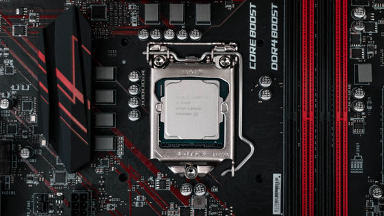
Intel announces plans to accelerate Moore's Law, aiming for 10x or more wiring density & up to 50% improvement in logic scaling
Gordon Moore, one of Intel founder has proposed 'integration density of the semiconductor has doubled 18 to 24 months, even if the performance of the chip is doubled advance further miniaturization' rule of thumb, that
Intel Breakthroughs Propel Moore's Law Beyond 2025
https://www.intel.com/content/www/us/en/newsroom/news/intel-components-research-looks-beyond-2025.html
Intel's Component Research Group is committed to 'new silicon capabilities to increase power and memory' and 'exploring new concepts in physics to revolutionize computing methods' in three key areas: Announced that it is working on innovation. Intel claims that innovations in three key areas will 'enable the evolution of semiconductors according to Moore's Law beyond 2025.'
Innovations in three key areas revealed by Intel are:
◆ 1: Intel is researching scaling technology that is indispensable for providing more transistors in future product offerings.
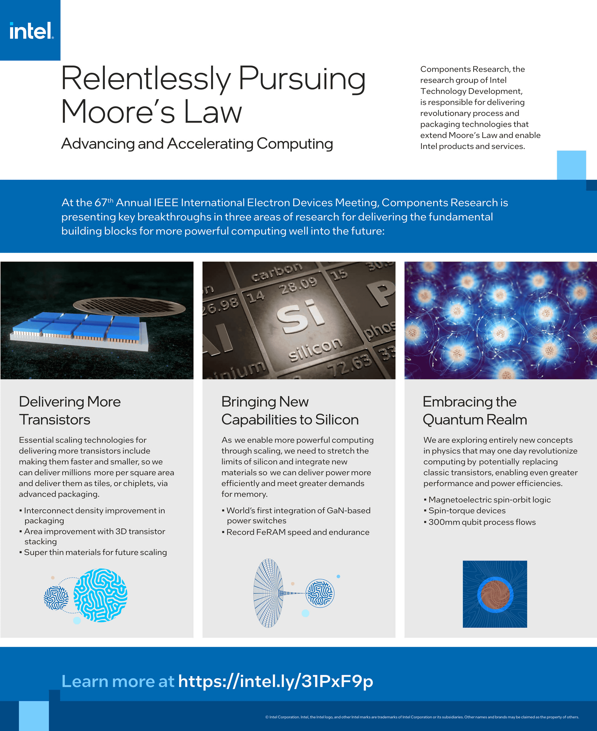
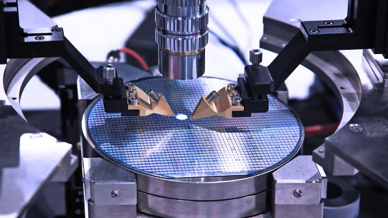
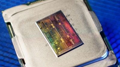
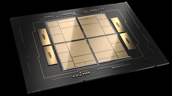
Intel researchers envision improving design, procedure, and assembly solutions for hybrid junctions and increasing interconnect densities in packaging by more than a factor of 10. Intel announces next-generation 3D packaging technology 'Foveros Direct' to achieve sub 10 micron bump pitch in order to achieve high interconnection density in 3D stacking. Intel says it wants to enable a hybrid bonding chiplet ecosystem to establish new industry standards and test procedures to enable the ecosystem to enjoy the benefits of advanced packaging.
Foveros Direct: Advanced Packaging Technology to Continue Moore's Law-YouTube
In addition, Intel is advancing the concept of MOSFETs to realize the continuous evolution of Moore's Law beyond the 'Ribbon FET', which is a field effect transistor (FET) with a GAA structure. Intel said it would respond to the post- FinFET era with an approach of stacking multiple CMOS transistors to enable up to 30-50% improvement in logic scaling. This allows you to install more transistors per square millimeter.
In addition, Intel is paving the way for Moore's Law to move into the Angstrom era, with the goal of adopting new materials that are only a few atoms thick. If this is achieved, it will be possible to overcome the limitations of traditional silicon channels and spread millions of transistors per die region.
◆ 2: Intel plans to add new features to silicon.
Intel is pursuing the world's first integration of CMOS silicon on 300mm wafers and GaN-based power switches as a more efficient power technology. If this is achieved, low-loss, high-speed power supply to the CPU will be possible, and space on the motherboard can also be reduced.
In addition, industry-leading low-latency materials with new ferroelectric materials for next-generation embedded DRAM technology to deliver increasingly complex computing applications from gaming to artificial intelligence (AI). We also aim to realize read / write functions.
◆ 3: Intel is pursuing massive performance in silicon transistor-based quantum computing, pursuing a whole new switch for highly energy-efficient computing with new room temperature devices. These technologies will use a whole new concept in physics in the future and may replace traditional MOSFET transistors.
Intel has successfully demonstrated the world's first experimental demonstration of a magnetic electric spin orbit (MESO) logic device at room temperature. Intel wrote about this, 'demonstrating the potential manufacturing potential of new types of transistors based on switching nanoscale magnets.'
In addition, Intel is collaborating with IMEC on research on spintronics materials, aiming to realize spin torque devices.
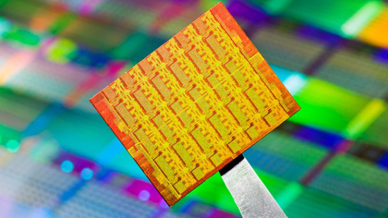
In addition, we are announcing a complete 300mm qubit process flow to enable scalable quantum computing that is compatible with CMOS manufacturing and is the next step for future research.
Intel, which announced various new information on semiconductor manufacturing, has also revealed that it plans to invest 30 billion rigs (about 800 billion yen) to build a new semiconductor packaging factory in Malaysia.
Related Posts:


in Hardware, Posted by logu_ii