TSMC announces that it will begin mass production of the 1.6nm generation semiconductor manufacturing process 'A16' by 2026
By
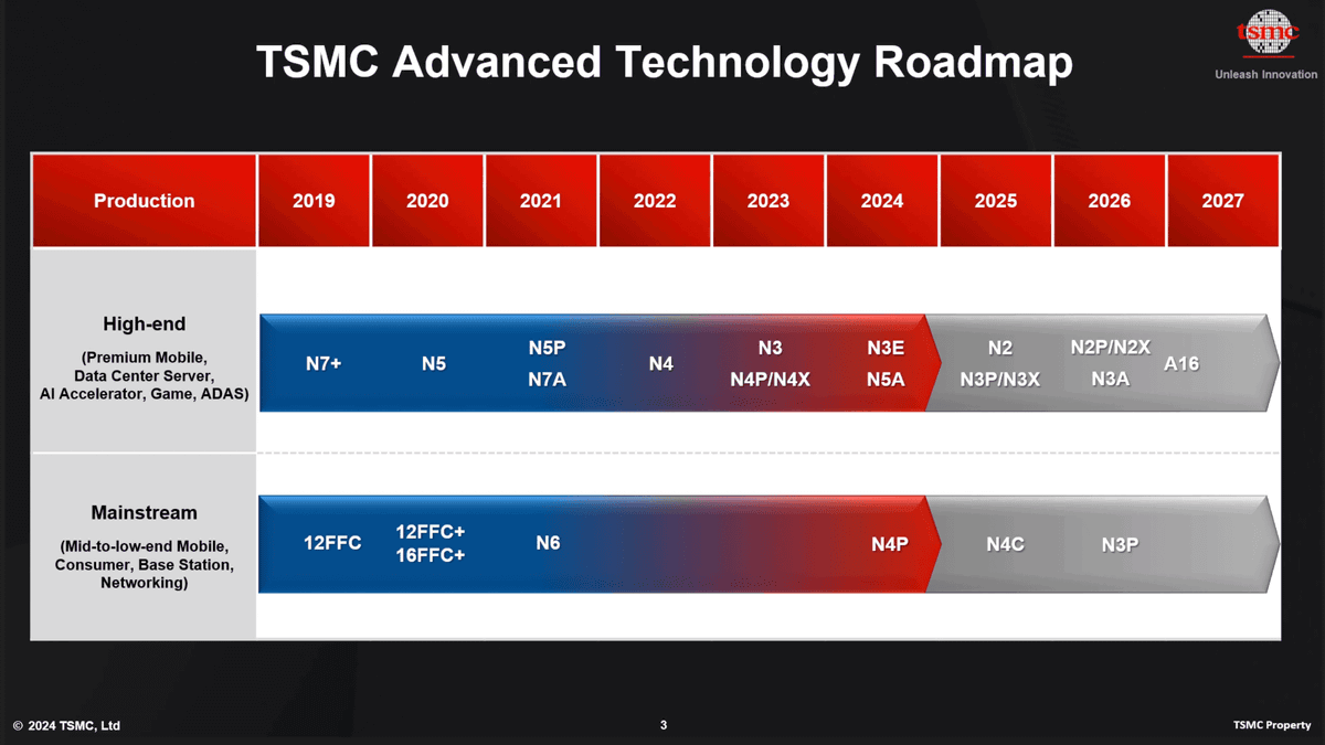
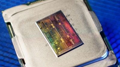
Semiconductor manufacturer TSMC announced at its symposium, North America Technology Symposium 2024 , held on April 24, 2024, that it plans to begin mass production of its 1.6nm generation semiconductor manufacturing process, A16 , in 2026.
TSMC Celebrates 30th North America Technology Symposium with Innovations Powering AI with Silicon Leadership
https://pr.tsmc.com/japanese/news/3136
TSMC unveils 1.6nm process technology with backside power delivery, rivals Intel's competing design | Tom's Hardware
https://www.tomshardware.com/tech-industry/tsmc-unveils-16nm-process-technology-with-backside-power-delivery-rivals-intels-competing-design
TSMC plans to begin mass production of the A16 process in 2026. The A16 will be the next-generation process following the 3nm generation 'N3E' process, which is already in mass production, and the 2nm generation N2 process, which will begin mass production in the second half of 2025.
TSMC officially announces expanded version of 3nm process and manufacturing technology of 2nm process, 2nm process will be launched in the second half of 2025 - GIGAZINE

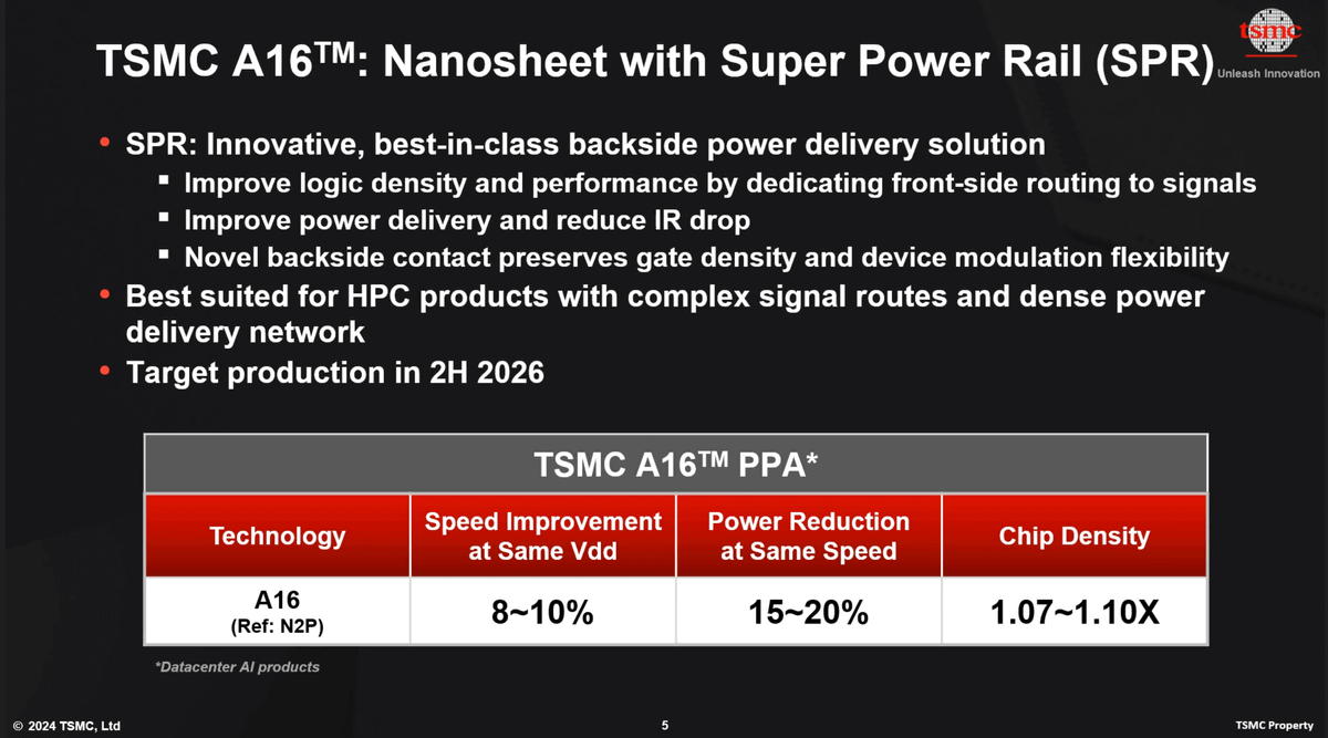
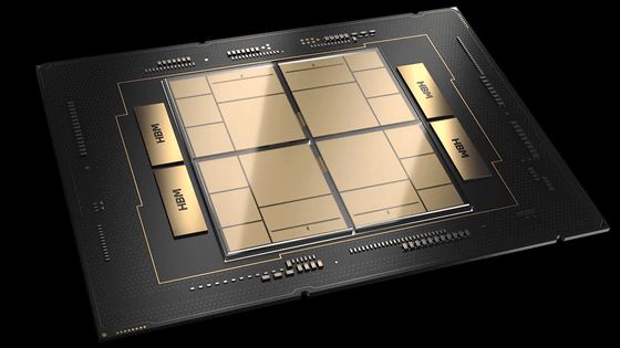
The A16 uses TSMC's cutting-edge 'nanosheet transistors.' Nanosheet transistors provide better electrical properties and controllability than conventional FinFET transistors, so performance and power efficiency can be improved while reducing the size of the transistor.
The A16 also features an architecture called 'Super Power Rail'. This Super Power Rail improves power supply performance by placing a dedicated power rail on the back of the chip. This allows the wiring resources on the surface to be specialized for signal wiring, which is advantageous for designs that require complex signal circuits.
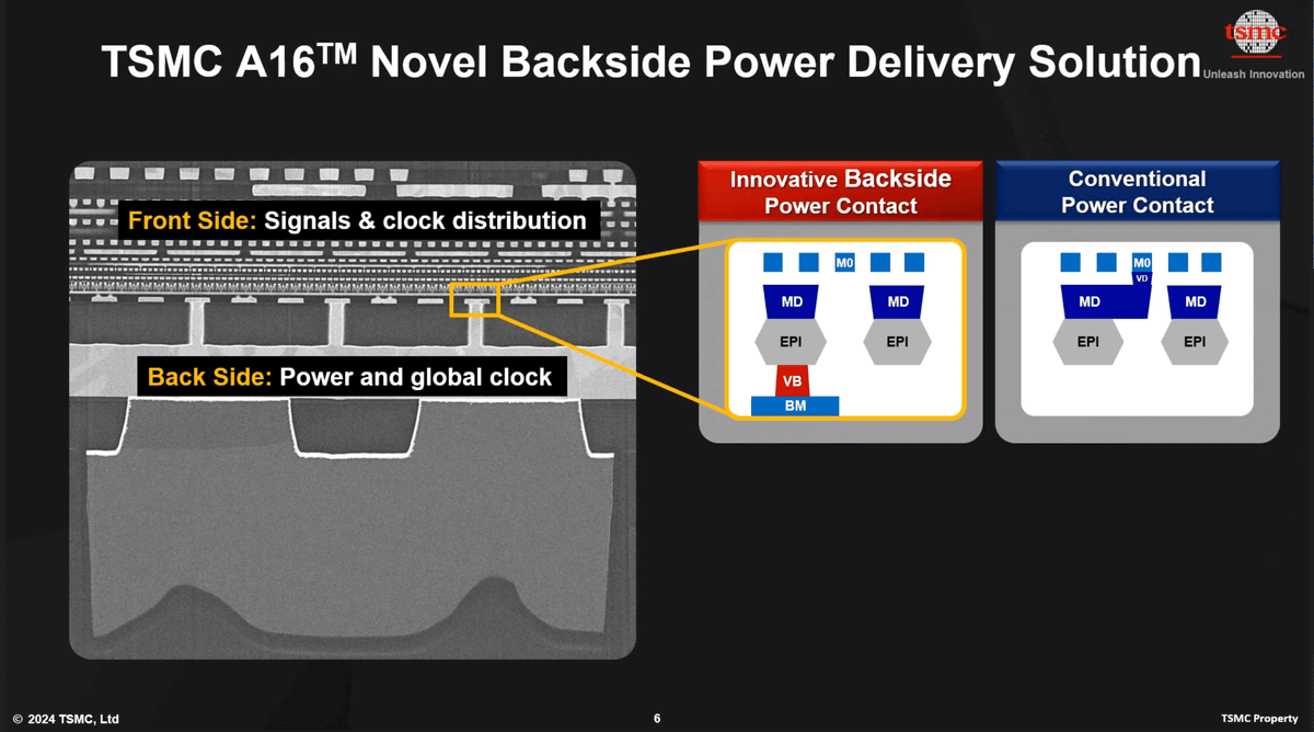
The A16 has a high-density power delivery network, making it suitable for power-hungry chips such as AI accelerators. According to TSMC, compared to the 2nm process generation N2P process, the A16 achieves an 8-10% speed increase at the same VDD (positive power supply voltage) and a 15-20% reduction in power consumption at the same speed, and it is said that chip density can be improved by up to 1.10 times in data center products.
TSMC also announced a technology called 'TSMC NanoFlex' that will be introduced to the N2 process. TSMC NanoFlex will have two types of standard cells for the N2 process: 'short cells' that aim for small area and excellent power efficiency, and 'tall cells' that aim for maximum performance. Chip designers can use many tall cells in design blocks that require high performance, and many short cells in parts that prioritize low power consumption, by combining short cells and tall cells within the same design block, and thus achieve optimal performance for each application.
In addition, TSMC has revealed that it plans to begin mass production of 'N4C', an extended version of the 5nm generation N4P process, in 2025. The point is that N4C adopts rules that are fully compatible with N4P, so the cost of transitioning from N4P to N4C is minimized. At the same time, N4C will achieve up to 8.5% die cost reduction compared to N4P, making it possible to manufacture chips with equivalent functionality at a lower cost compared to N4P. TSMC says that this cost reduction will be achieved by improving yield rates due to the reduction in die size.
TSMC also announced 'CoWoS (Chip on Wafer on Substrate)', which arranges multiple processor cores and High Bandwidth Memory stacks side by side, 'SoIC (System on Integrated Chips)', which realizes a high-density, high-performance system by stacking multiple chips vertically, and 'TSMC-SoW (System-on-Wafer)', which arranges a large-scale die array on a 300 mm wafer. All of these are advanced packaging technologies for designing higher density and higher performance SoCs.
TSMC is developing a technology called COUPE (Compact Universal Photonic Engine) to support the explosive increase in data transmission accompanying the AI boom. COUPE is a silicon photonics integration technology that stacks electrical dies on top of photonic dies through 'SoIC-X chip stacking' to provide the lowest impedance at the die-to-die interface and improve energy efficiency compared to traditional stacking methods. COUPE is expected to be integrated with CoWoS in 2026 and offered as CPO (Co-Packaged Optics).
TSMC also announced 'InFO-oS' and 'CoWoS-R' as technologies for automobiles. Both are adaptations of TSMC's advanced technologies for automobiles, and the company aims to obtain AEC-Q100 Grade 2 certification by the fourth quarter of 2025.
'We are entering a world where AI will not only run in data centers, but also in PCs, mobile devices, automobiles and even the Internet of Things,' said TSMC CEO Xi Xi Wei. 'At TSMC, we offer the most comprehensive range of technologies to help our customers realize their AI vision - from the world's most advanced silicon to the broadest portfolio of advanced packaging and 3D IC platforms, to specialized technologies that converge the digital and physical worlds.'
◆ Forum is currently open
A forum related to this article has been set up on the official GIGAZINE Discord server . Anyone can post freely, so please feel free to comment! If you do not have a Discord account, please refer to the account creation procedure article to create an account!
• Discord | 'What device has the smallest process semiconductor among all the devices you own?' | GIGAZINE
https://discord.com/channels/1037961069903216680/1233343036541374514
Related Posts:


in Hardware, Posted by log1i_yk