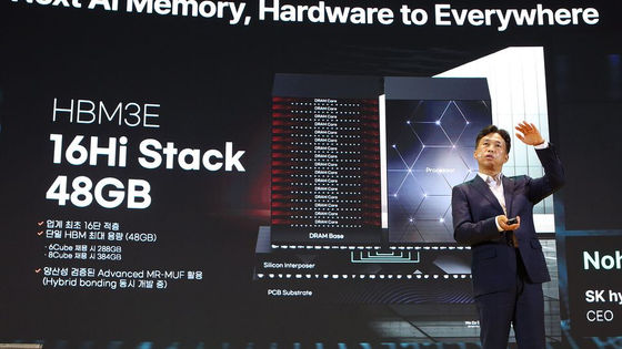
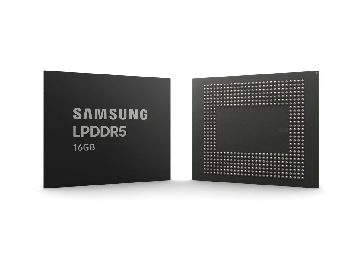
Samsung starts mass production of mobile 16Gb LPDDR5 DRAM adopting 3rd generation 10 nm process
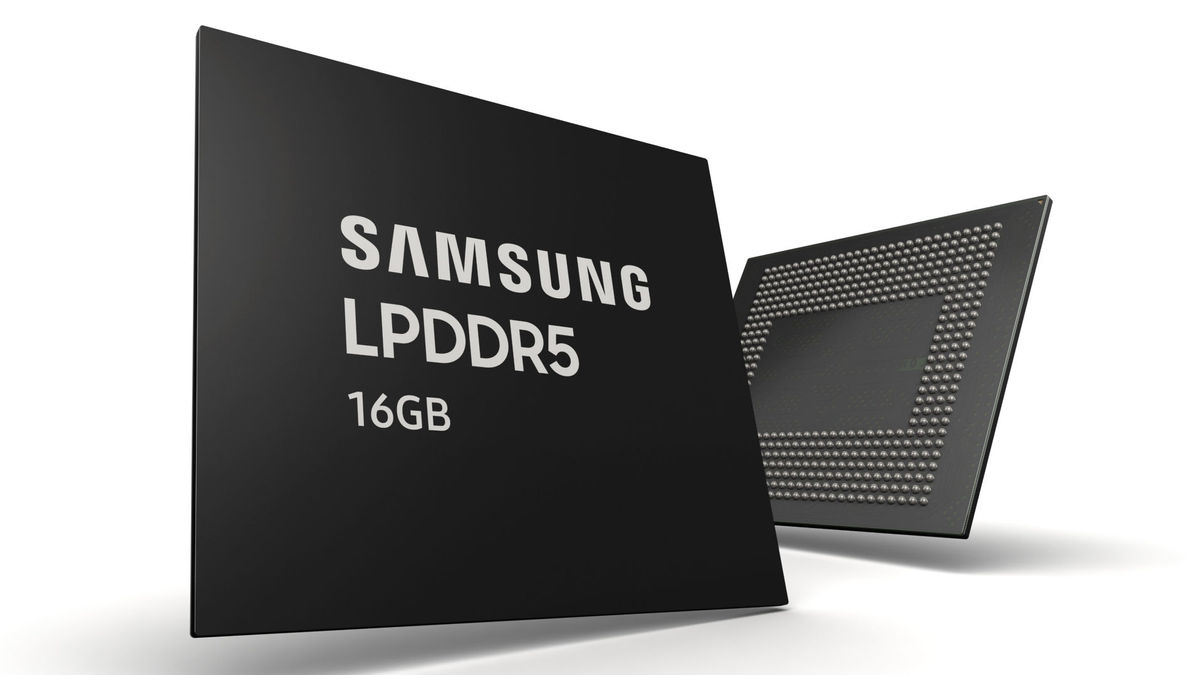
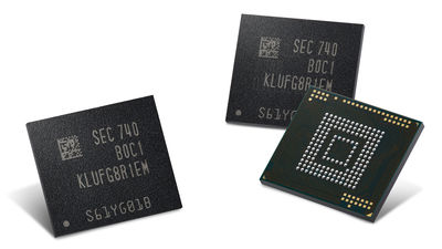
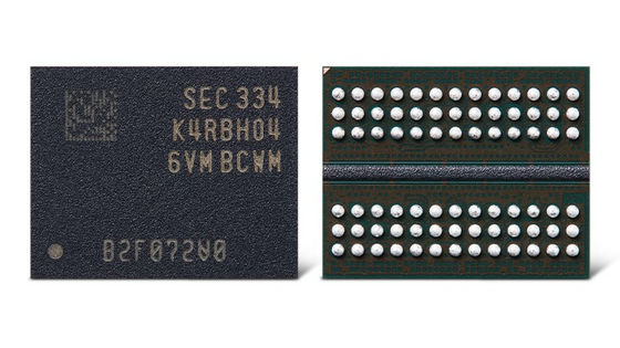
Samsung announced that it has started mass production of its 16Gb (Gigabit) LPDDR5 DRAM for mobile devices using the 3rd generation 10nm process.
Samsung Begins Mass Production of 16Gb LPDDR5 DRAM at World's Largest Semiconductor Line – Samsung Global Newsroom
Samsung starts mass producing 16Gb LPDDR5 DRAM chips at Pyeongtaek plant-SamMobile
https://www.sammobile.com/news/samsung-starts-mass-production-16gb-lpddr5-dram-chips-pyeongtaek-line-2/
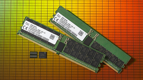
Samsung has started mass production of a 16Gb DRAM chip that uses EUV lithography and adopts the third generation 10nm process. According to the company's official announcement, this 16Gb DRAM chip combines not only mobile memory capacity but also performance, and the data transfer rate is 6400 Mbps, which is 16% faster than the 12Gb LPDDR5 DRAM chip installed in today's flagship mobile devices. It has reached. A device equipped with a 16GB package consisting of 16Gb LPDDR5 x 8 chips will be able to transfer 51.2GB of data in 1 second.
In addition, the 16Gb LPDDR5 chip has achieved a space saving of 30% reduction by the 3rd generation 10nm process compared to the conventional product that adopted the 2nd generation 10nm process of the same company. The LPDDR5 DRAM chip is expected to be used for in-vehicle devices as well, and Samsung says it 'provides temperature range and reliability standard for harsh environments.' Samsung plans to mass-produce the new 16Gb LPDDR5 chip to further strengthen its presence in the flagship mobile device market in 2021.
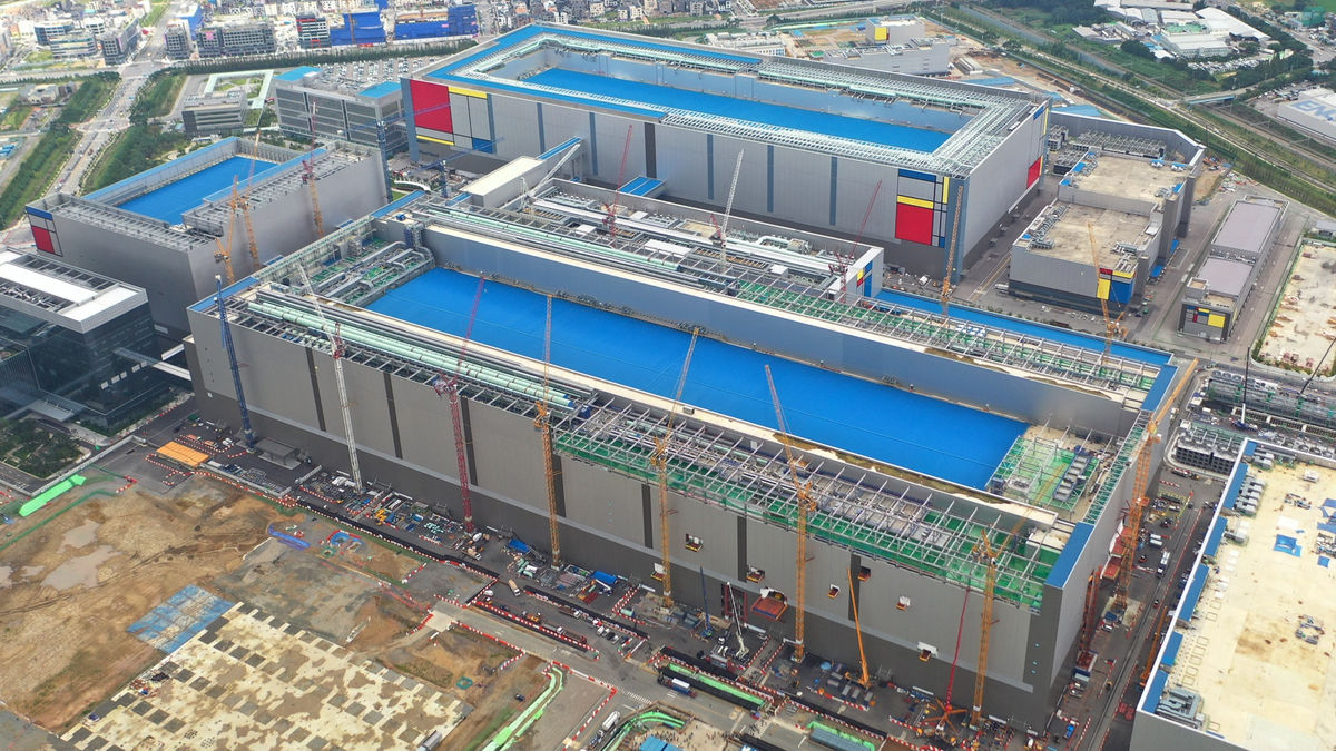
The production line for this 16Gb LPDDR5 chip will be the second production line of the Hirasawa Plant, which is the largest semiconductor production line and covers 129,900 square meters. The second production line of the Hirasawa Plant will function as a major manufacturing hub for the industry's most advanced semiconductor technology, and will be used not only for the most advanced DRAM, but also for the production of next-generation V-NANDs and foundry solutions.
Jung-Bae Lee, Vice President of Samsung's DRAM Project & Technology Division, said, 'The new 3G 10nm process 16Gb LPDDR5 overcomes the DRAM size problem in advanced nodes and sets new boundaries for the industry. We will continue to exceed customer demand by expanding our premium DRAM line-up while leading the growth of the overall memory market.'
Related Posts: