'ChipTycoon' is a game-like visual and explanatory game that makes it easy to understand how semiconductors are made.

' Chip Tycoon ,' an animated visualization of the semiconductor manufacturing process, has been released. You can understand the manufacturing process by watching semiconductors move around in a miniature factory.
ChipTycoon: How a Computer Chip Is Made
When you access Chip Tycoon, you'll see a semiconductor factory. The manufacturing process is divided into 20 stages, with carts transporting semiconductors to each facility. Semiconductors begin with ordinary sand. But not just any sand; it's quartz sand containing a very high amount of a mineral called silica. Silica is a compound of silicon and oxygen, and since about a quarter of the Earth's crust is made up of silicon, there's no need to worry about running out of raw materials. The highest quality quartz is mined from limited mines and has a white, glass-like appearance even before processing.
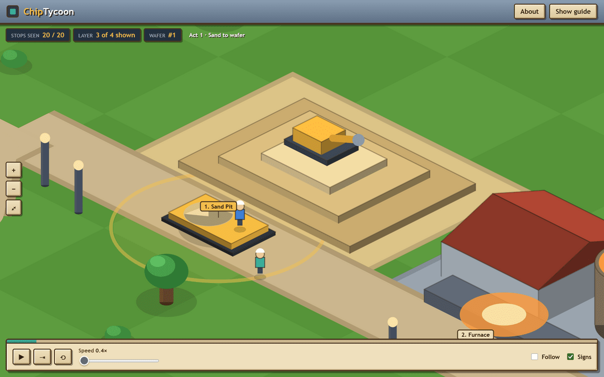
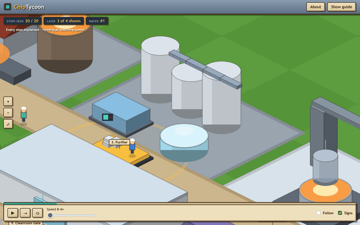
Next, quartz sand and carbon are placed in a huge electric furnace at approximately 2000°C. Because carbon strongly attracts oxygen, it removes oxygen from the sand, and the oxygen escapes as a gas. Flowing out from the bottom of the furnace is molten silicon with a purity of approximately 99%. 99% may seem sufficient, but the goal is 99.9999999%. The next building's role is solely to remove the remaining impurities.

In the next facility, the gas is repeatedly distilled to remove impurities. Then, the purified gas is poured onto a high-temperature rod, causing silicon to precipitate as a solid on the surface. This is how polysilicon is produced, with a purity of 99.9999999%. It's like having just one grain of sugar mixed in with a pool full of sugar.
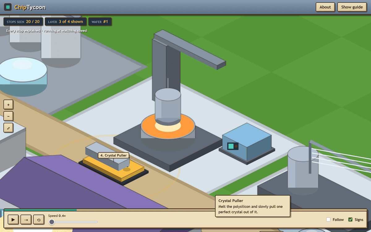
Polysilicon is a collection of tiny crystals orienting in various directions. However, in semiconductors, all atoms must be arranged in the same regular lattice pattern. To achieve this, polysilicon is melted, a small seed crystal is immersed in it, and then it is slowly pulled up while rotating. The silicon then freezes onto the seed crystal, copying its crystalline structure exactly. After being pulled up for one to two days, a silvery cylinder measuring 2 meters in length and weighing several hundred kilograms is formed. The entire cylinder, from end to end, is a single crystal.
Next, the crystal is sliced into thin discs, like salami. Hundreds of thin slices are made at once using a wire saw with many thin wires coated with diamond particles. Each slice is a wafer. They are less than 1 mm thick and look like dull gray discs. They are made slightly thicker than the actual required thickness to prevent them from breaking when transported by robots.

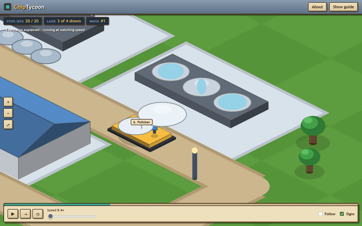
Using a rotating polishing pad and a milky white polishing liquid, the surface is polished roughly at first, and then very carefully. The finished wafer is like a mirror. Even if you were to enlarge it to the size of a soccer field, the highest point would only be about the height of a coin. This level of flatness is necessary because light will be used to draw circuits later. If the surface is uneven, the light cannot be kept focused.
A semiconductor is like a road map, composed of billions of tiny switches called transistors and the wiring that connects them. Of course, it's not drawn by hand, one by one; instead, a special design language is used to describe 'what we want this semiconductor to do,' and software automatically creates the layout. The completed design is divided into multiple layers, like the floors of a building, and each layer represents one printing stage in the subsequent process.
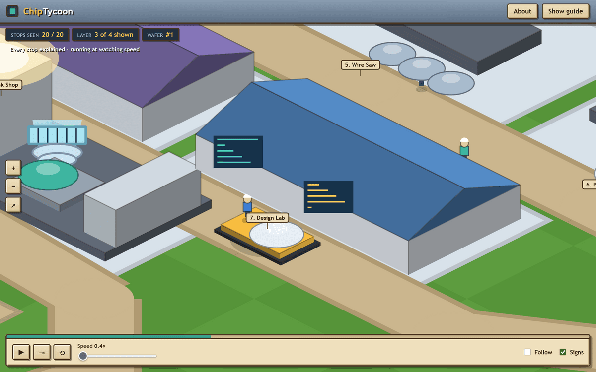
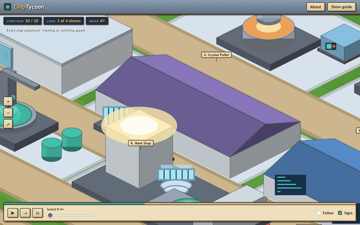
Each layer of the design becomes a glass master called a mask. A mask is a very high-purity glass plate onto which a single layer of circuit pattern is drawn using a thin metal film. Light passes through only the transparent parts, while the metal parts block light. Typically, more than 60 masks are needed for a single semiconductor design. The patterns drawn on the masks are made about four times larger than the finished semiconductor. The exposure equipment then reduces them and prints them.
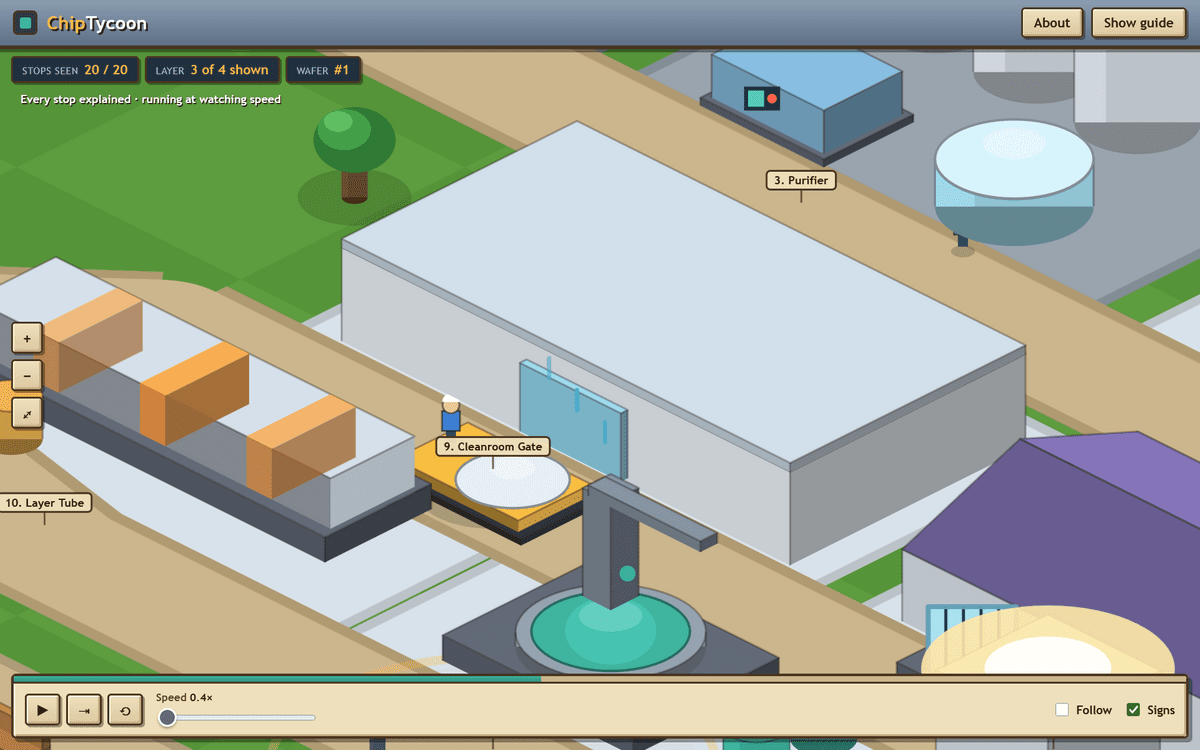
From this point onward, the process takes place in an environment with air even cleaner than that of an operating room. The structures that will be printed are far smaller than a single grain of dust, so if even one grain of dust falls onto the wafer, the semiconductor underneath will be rendered unusable. By pushing in air filtered through microscopic filters from the ceiling and drawing it out from the floor, dust has no time to accumulate. The reason why workers wear full-body white protective suits is not to protect themselves, but to protect the wafers from people. This is because people are constantly shedding skin cells and hair.
Next, the entire wafer is uniformly covered with a thin film. When the wafer is heated in oxygen, the silicon surface changes to glass (oxide film), which becomes an excellent insulator. Sometimes, a method is used in which gases adhering to the surface are blown in, and metals and insulators are stacked up one atom at a time. These thin films are surprisingly thin, some of which are only a few atoms thick. At this point, the film uniformly covers the entire wafer, but it has not yet taken on the desired shape.

A liquid called 'photoresist,' whose properties change with light, is applied to the wafer. A few drops are placed in the center of the wafer and it is rotated at high speed, causing the liquid to spread uniformly due to centrifugal force. Photoresist has properties similar to old camera film, and only the parts exposed to light change. Therefore, this entire process is carried out under yellow lighting. This is why some photographs of semiconductor factories have a yellowish atmosphere.

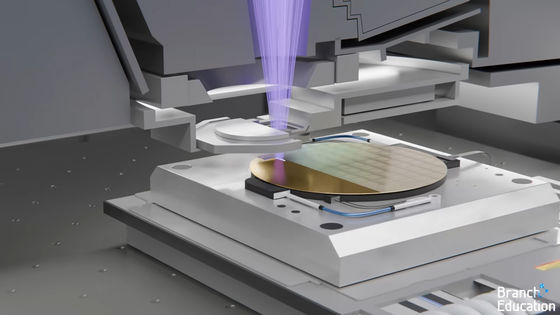
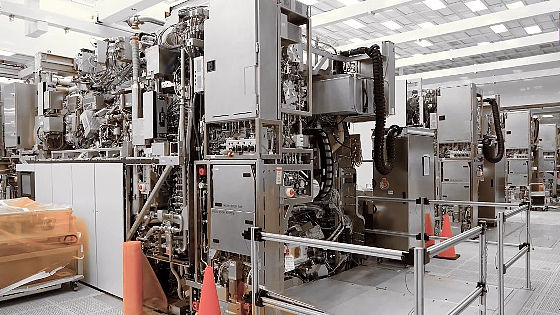
This is the heart of the factory. Circuit patterns are imprinted onto wafers as shown in the photograph. Light is passed through a mask, and the image is reduced by multiple lenses before being shone onto the wafer coated with photoresist. Only the photoresist that is hit by the light changes, while the shaded areas remain unchanged. Since only a small area can be exposed at a time, the wafer is moved slightly to the side after exposure and exposed again. This process is repeated many times to imprint hundreds of the same semiconductors onto the entire wafer. EUV (extreme ultraviolet) is used for the finest patterns. EUV is extremely difficult to handle and is absorbed not only by ordinary glass but also by air, so the equipment operates in a vacuum and the light is controlled using mirrors instead of lenses.

Next, the altered photoresist is washed away, and the layer beneath is removed. A liquid is used to wash away only the photoresist that has been altered by the light, leaving the photoresist itself as a template. This is followed by etching. Plasma removes only the exposed parts, without touching the parts covered by the photoresist. Finally, the remaining photoresist is removed, and the circuit pattern is etched into the actual layer.

Pure silicon does not conduct electricity very well. However, by adding tiny amounts of other elements such as boron or phosphorus, its conductivity can be controlled at will. Ion implanters accelerate these atoms to very high speeds and fire them into the wafer like a paint spray gun.

Next comes the wiring process. Grooves are cut into the insulating film, and then the entire surface is covered with copper, which fills the grooves. Then, the excess copper is polished away, leaving copper only in the grooves. That is the wiring. Another insulating film is formed on top of that, and the same process is repeated. In modern semiconductors, dozens or more layers of wiring are stacked on top of each other. If you were to stretch out all the internal wiring in a single large processor the size of a postage stamp in a straight line, it would stretch for tens of kilometers.

This completes one layer. Since actual semiconductors have about 60 layers, the last six steps are not a one-time process but are repeated for months. After forming a layer, applying photoresist, exposing it, etching, doping or forming wiring, and polishing it flat, the same process is repeated for the next layer. This is why it takes about three months to manufacture a semiconductor and why wafers travel many kilometers around the factory before completion. It's not waiting for a single process to finish, but rather repeating the same process over and over again.

The finished wafers are inspected. A thin needle is touched to the small metal pads of each semiconductor, a test signal is sent, and the return result is checked. Defective products are marked. In a normal manufacturing line, most semiconductors pass, but not all of them pass. This pass rate is called the yield. The yield is the number that determines whether a semiconductor factory will make a profit or incur a loss.
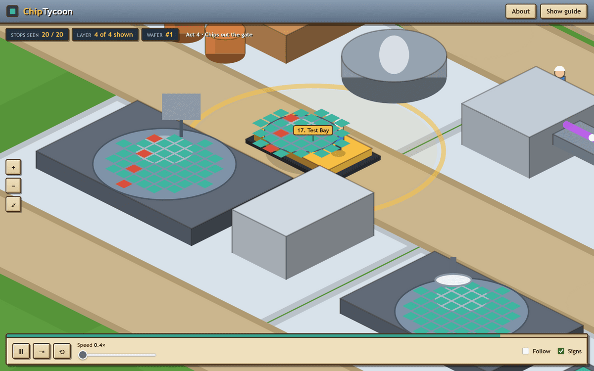
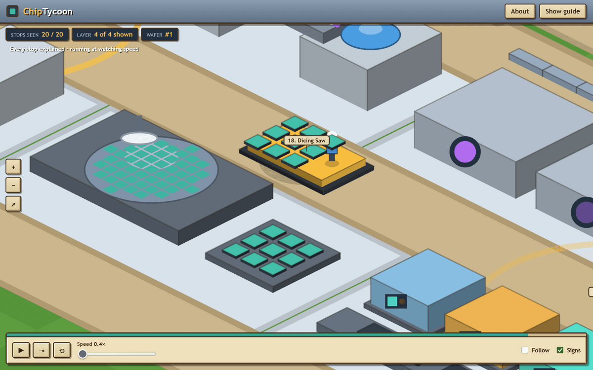
Next, the circular wafer is cut into hundreds of tiny squares. Using diamond blades or lasers, the wafer is cut along narrow gaps that were pre-designed between the semiconductors during the design phase. Each separated piece is called a die, and it is thinner than a fingernail. Only the dies that pass the inspection are collected, while those deemed defective are discarded. Although the wafer is circular, the semiconductors that are cut are square, so the edges of the wafer are always wasted. The larger the wafer, the smaller the waste, so the industry continues to move towards larger wafers.
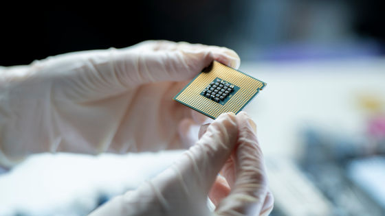
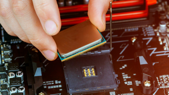
Because exposed dies are too fragile, they are placed in a case. The die is glued to a small circuit board and connected to metal terminals on the board with wires as thin as a strand of hair or tiny solder balls. Then, it is covered with a metal lid or a hard plastic case. The black rectangular components visible on the semiconductor circuit board are not the semiconductor itself, but the package. The package serves to spread out the terminals to make wiring easier on the circuit board, and also plays a role in dissipating heat.

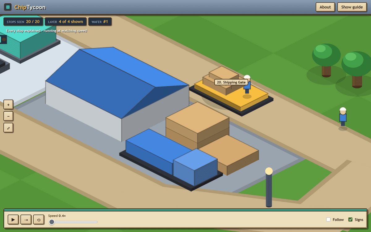
Final testing is conducted, and the semiconductors are sorted according to their performance before shipment. Here, semiconductors are tested at high and low temperatures and at their maximum operating speed. This is because a semiconductor that functions normally on a workbench may not work properly inside a warm laptop. The grade is determined by the test results, with the fastest and most reliable ones sold in the highest price range, and the rest assigned to lower-priced models. After that, they are packed into trays or reels, transported by air, and sent to factories where they are soldered onto printed circuit boards.
Related Posts:

in Hardware, Posted by log1p_kr