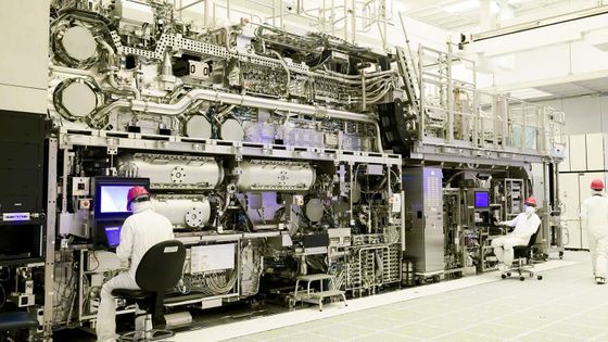
What exactly is the mechanism behind 'EUV lithography,' a manufacturing device that packs tens of billions of tiny transistors into a small CPU?
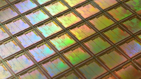
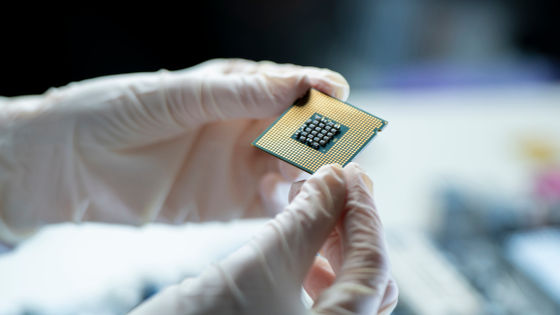
Existing high-tech devices, such as laptops, smartphones, and AI servers, are built with cutting-edge semiconductors. These devices contain tens of billions of
How are Billions of Nanoscopic Transistors Made into a Microchip? EUV Photolithography 🛠⚙️🤯 - YouTube
Branch Education describes EUV lithography as a 'nanoscale copier.' Here's a simple explanation of how it works:
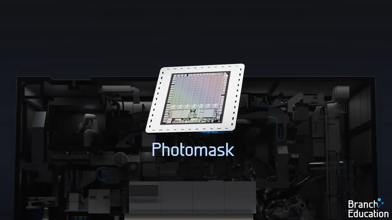
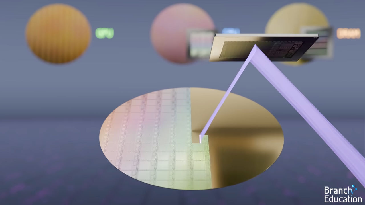
1: The design data for one layer of a chip is recorded on a plate called
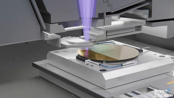
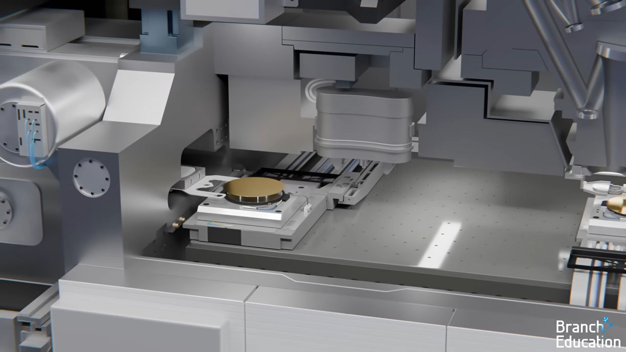
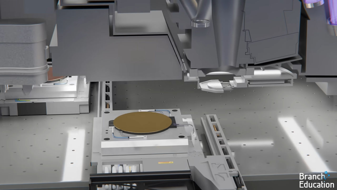
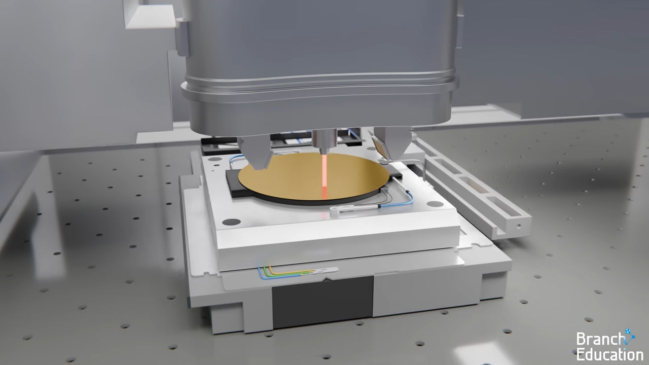
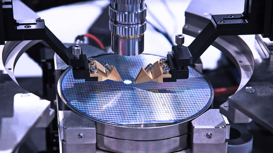
2: Place a 300mm
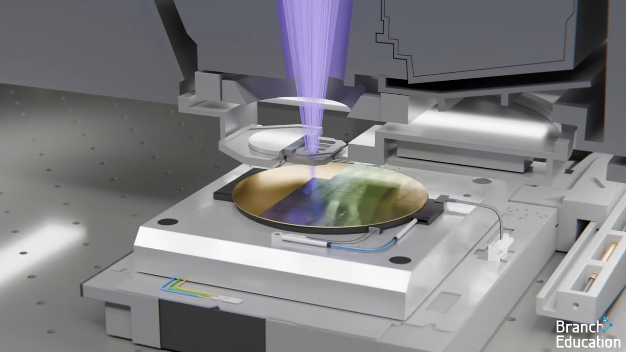
3: The device uses a combination of extreme ultraviolet (EUV) light and mirrors to transfer the design on a photomask onto a wafer.
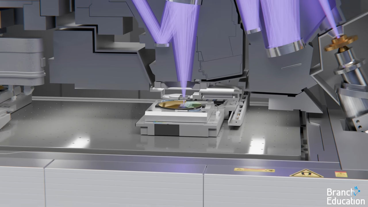
4: The same pattern is copied multiple times while moving the wafer slightly.
5: Once more than 100 microchips have been transferred onto one wafer, the next wafer is inserted.
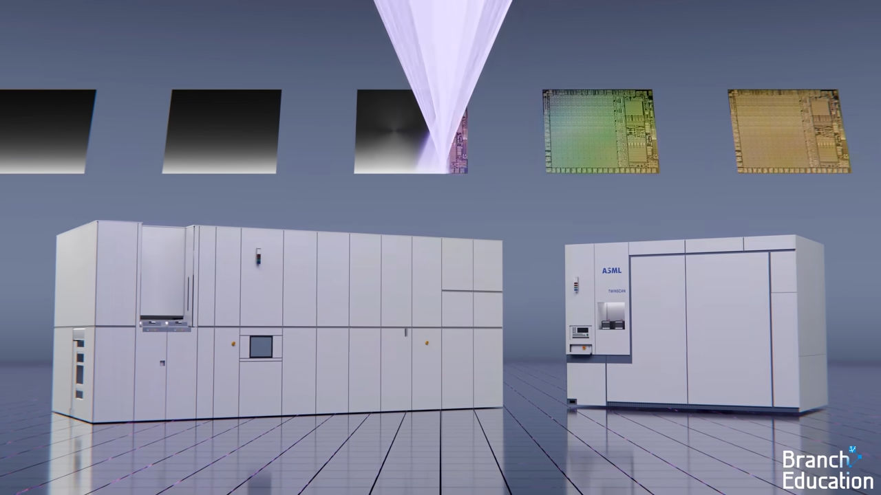
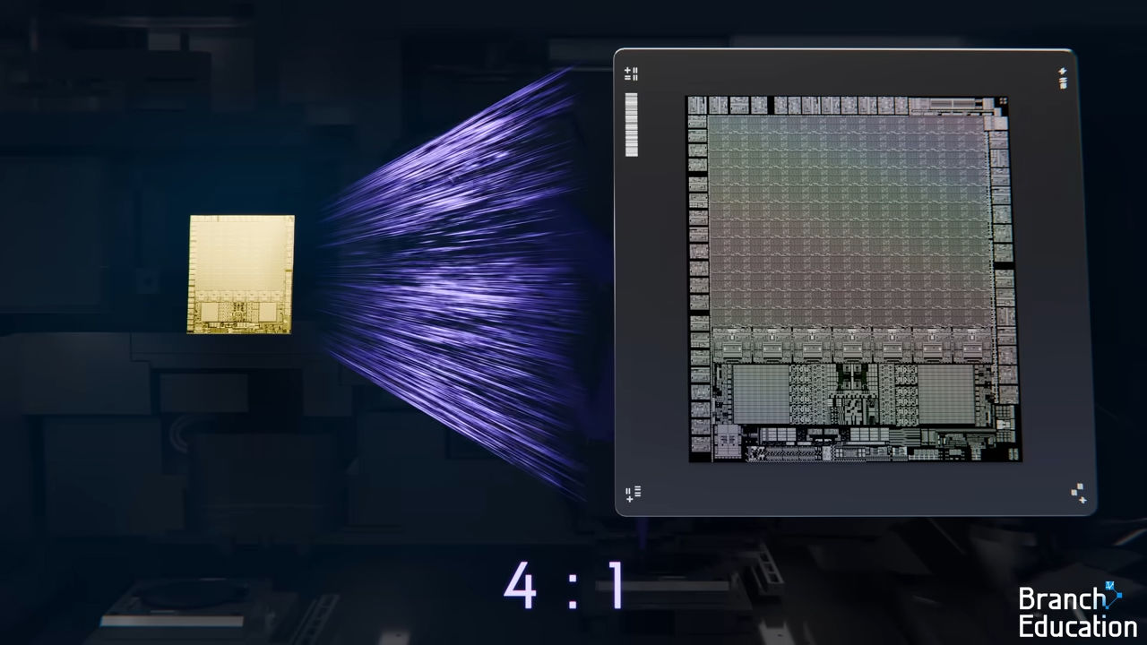
EUV lithography can replicate the same chip approximately 100 times on a single wafer in approximately 18 seconds. For example, a GPU contains approximately 30 billion transistors, but at the nanoscale, they are made up of multiple layers of interconnects and transistors arranged in a three-dimensional structure, with the smallest part measuring just 10 nm.
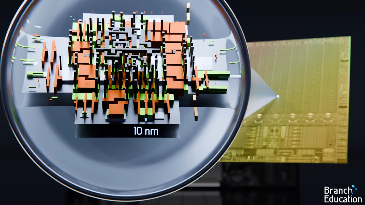
EUV lithography is used to form the fine patterns on the bottom layer, while a separate exposure tool is used for the larger patterns on the upper layers. Assuming EUV lithography can print text, the width of each line is 13 nm, so the word 'Cat' would only measure about 155 x 240 nm. If text were written using EUV lithography, even a page of text printed using a novel would only be about the size of a red blood cell.

An area the size of a typical GPU chip could easily print an entire library collection, and EUV lithography can copy this vast amount of information in less than a second. Branch Education noted that 'it's no exaggeration to say that all modern technology is made possible by this device.'

EUV lithography begins with generating extreme ultraviolet light. Extreme ultraviolet light has a wavelength of 13.5 nm (about 1/15 of visible light), and producing light with such a short wavelength was an extremely difficult technical challenge.
The process by which ASML's EUV lithography produces extreme ultraviolet light is as follows: Simply put, a laser is fired at liquid tin to create a glowing plasma, a process that is repeated more than 50,000 times per second.
1: Tiny droplets of tin (approximately 25 micrometers in diameter) are sprayed into a vacuum at high speed.
2: The droplets are flattened by applying a laser pulse.
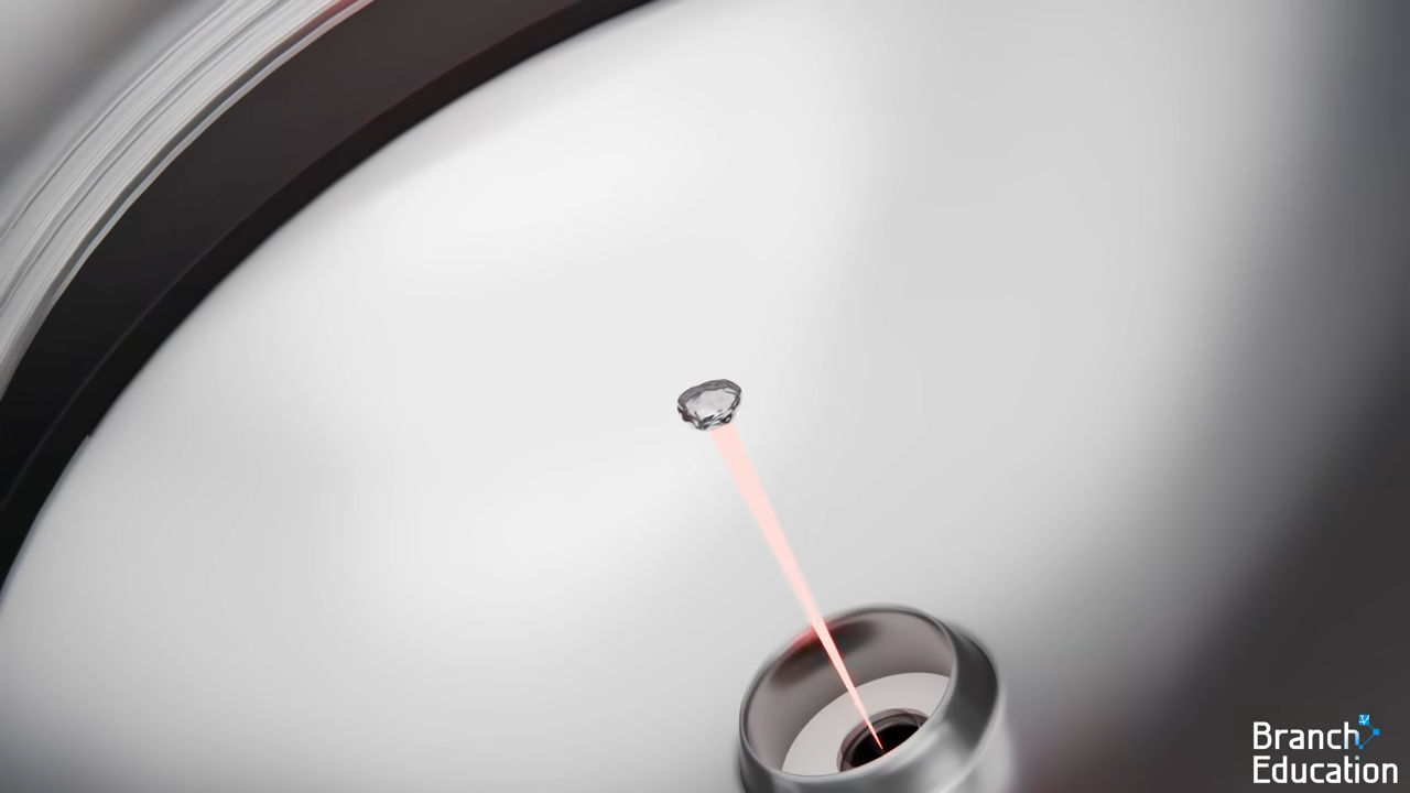
3: A powerful laser pulse hits the droplets, transforming them into a plasma state at approximately 220,000 degrees.
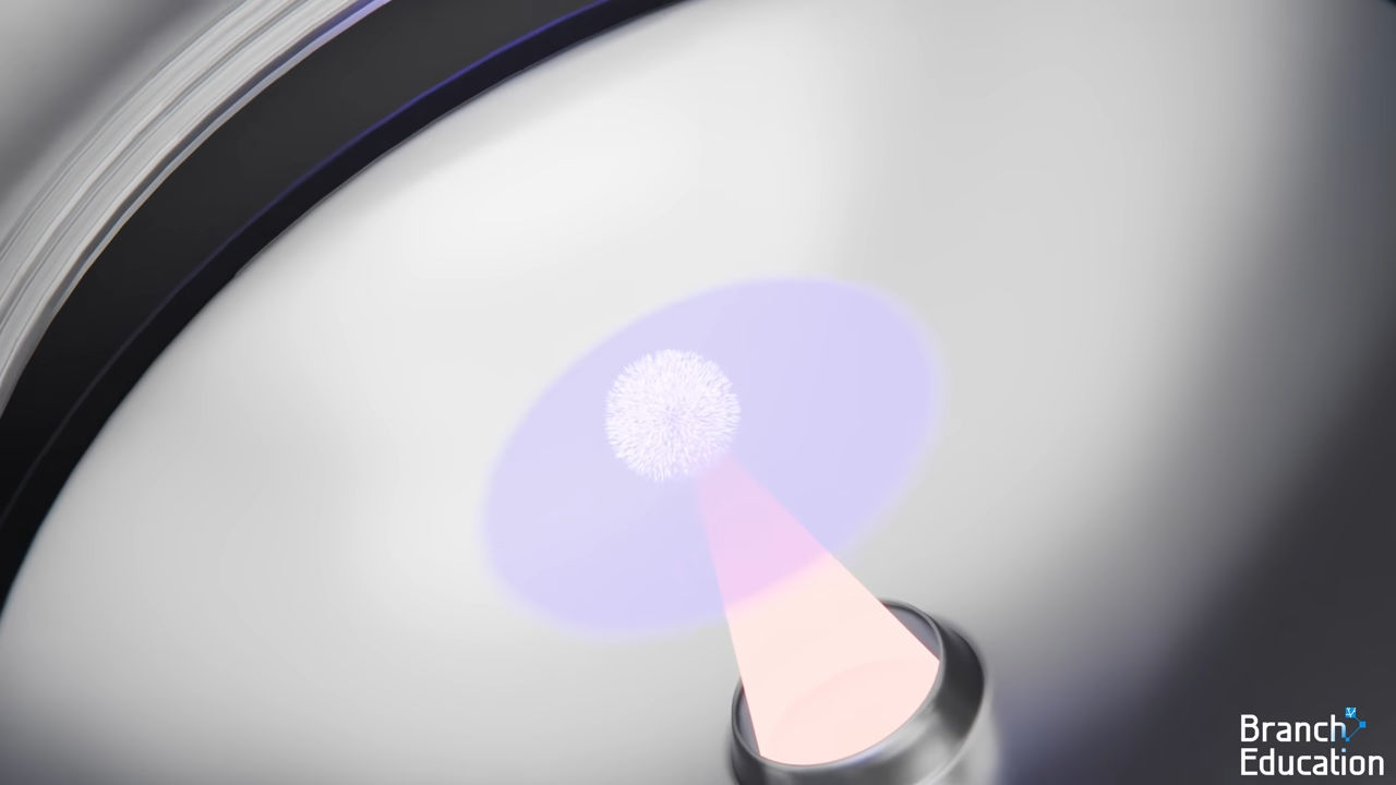
4: This plasma emits EUV light (violet).
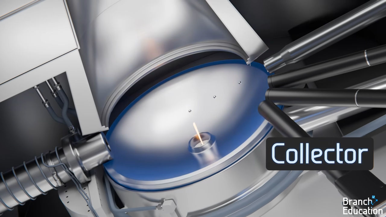
The generated EUV light is emitted in all directions, so it needs to be collected efficiently. This is where the collecting mirror (shown in blue) comes in. The collecting mirror is designed to direct the EUV light to the next optical module in the device, but because EUV light is quickly absorbed in air, the entire device is designed to operate in a complete vacuum environment. It should be noted that even a small amount of oxygen or nitrogen will cause the EUV light to disappear.
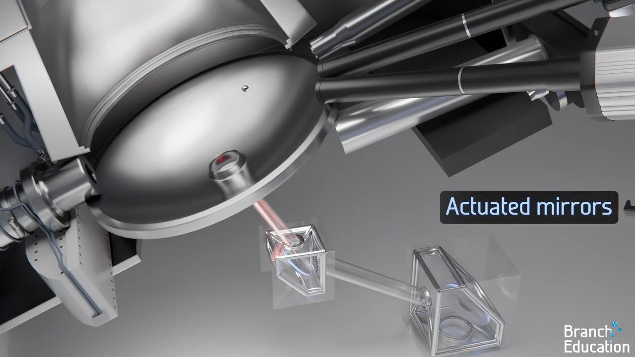
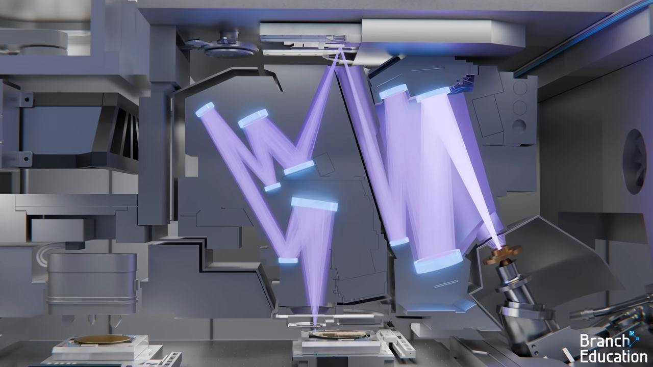
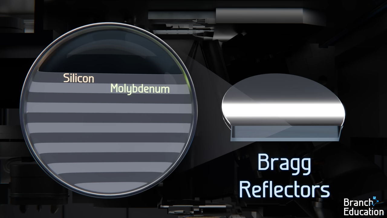
There are no lenses that can refract EUV light because EUV light cannot penetrate any glass. Therefore, all EUV lithography uses mirrors to reflect and control the light, and ASML's EUV lithography uses high-precision mirrors developed by
This mirror is made up of over 100 alternating layers of
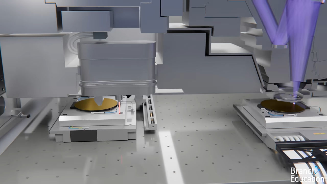
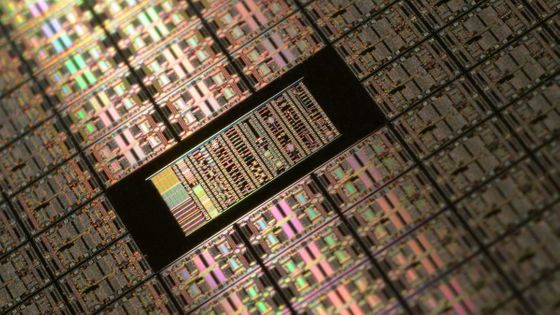
The EUV light collected by the mirror enters the illumination optical system, where the shape and uniformity of the light are adjusted and controlled so that it is accurately irradiated onto the photomask. The photomask contains the circuit pattern for one layer of the chip, and for EUV, a reflective photomask is used instead of a transmissive one. The surface of the photomask has reflective and absorbing areas, and the light is reflected to transfer the chip design.
Because the circuit pattern on the photomask is transferred hundreds of times, even the slightest defect will be copied hundreds of times on the wafer. Therefore, the surface precision of the wafer must be inspected at the atomic level, and electron beam scanners and interferometers are used to detect defects.
The EUV light reflected by the photomask is reduced through a projection optical system and projected onto a silicon wafer. The projection magnification is about 1/4. A pattern of 1 mm on the mask is reduced to 0.25 mm on the wafer. This reduction is made possible by a group of six high-precision mirrors made by Carl Zeiss. Each of these mirrors has a surface error of only a few atoms, and their shape is adjusted to the nanometer level.
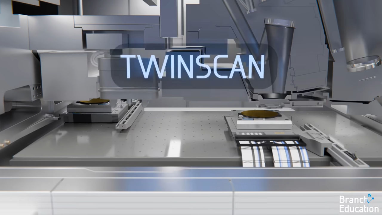
One of the most amazing mechanisms in EUV lithography is
To achieve this level of precision, the wafer stage is operated by a linear motor and uses
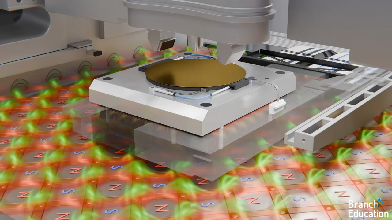
This is made possible by ASML's proprietary TwinScan, which allows for parallel operation: 'While exposure is performed on one stage, the next wafer is measured and prepared on the other stage.' This has apparently dramatically improved processing speed.
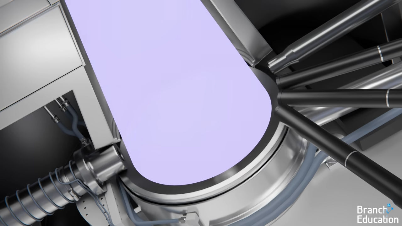
Because EUV light dissipates in air, the entire exposure process takes place in a high-vacuum chamber. However, the chamber can produce residual tin particles and contaminate the mirror surface. ASML's EUV lithography system incorporates a magnetic filter and mirror-cleaning laser to remove the tin particles. Without these maintenance mechanisms, the mirror's reflectivity would deteriorate in just a few days.
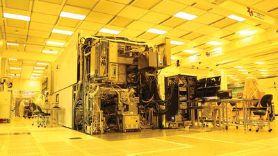
EUV lithography is essentially a 'giant robot with nanoscale precision.' Each machine is equipped with over 100,000 sensors that provide real-time feedback control. Optical, thermal, and mechanical parameters are linked between each module, and hundreds of CPUs,
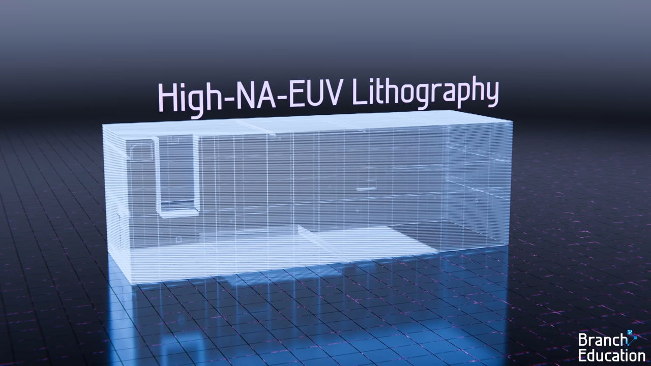
At the time of writing, EUV lithography is primarily used in chip manufacturing for the 3nm to 2nm generations. However, as transistors continue to shrink, moving toward the 1.4nm and 1nm generations, the physical limits of EUV's 13.5nm wavelength are approaching. Therefore, high-NA EUV (high numerical aperture EUV) is gaining attention as the next step. This method increases optical magnification and further improves resolution, and is used in conjunction with EUV double exposure and nanoimprint technology. Research is also underway on soft X-ray lithography and electron beam direct writing for the future.
Related Posts:

in Video, Posted by logu_ii