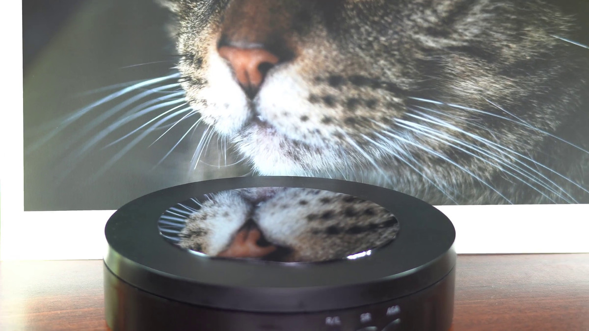
A movie that shows 'how to make a CPU' in just 99 seconds
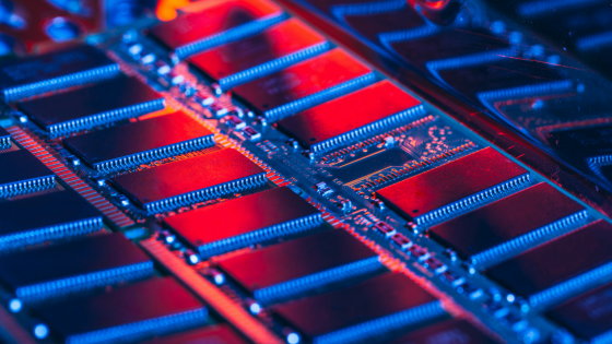
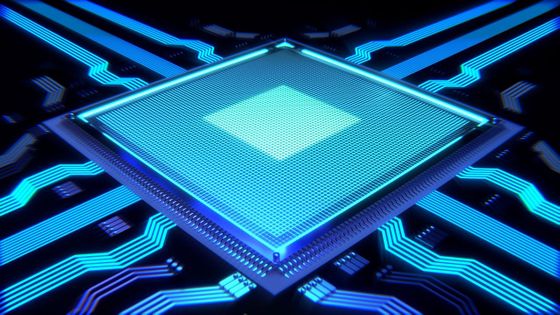
Computers and electric appliances that incorporate computers, such as PCs and smartphones, which are indispensable in the daily lives of modern people, are equipped with semiconductor chips called CPUs (Central Processing Units) and GPUs (Graphics Units).
Man Solves Global Chip Shortage In 99 Seconds --YouTube
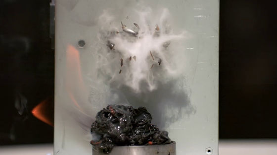
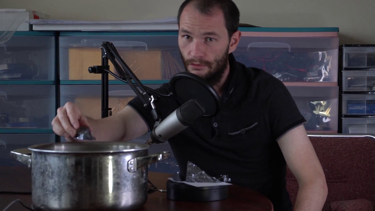
First, pick up the stone.
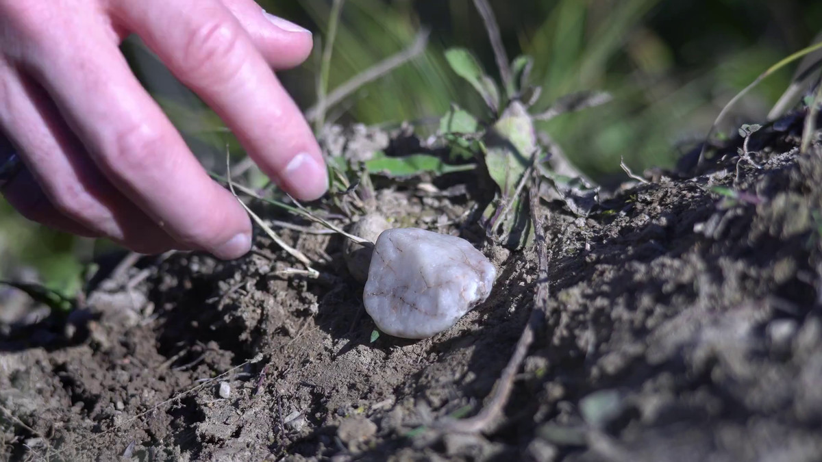
Crush the picked stones into pieces.

Then, silicon dioxide with a purity of 98% was produced.
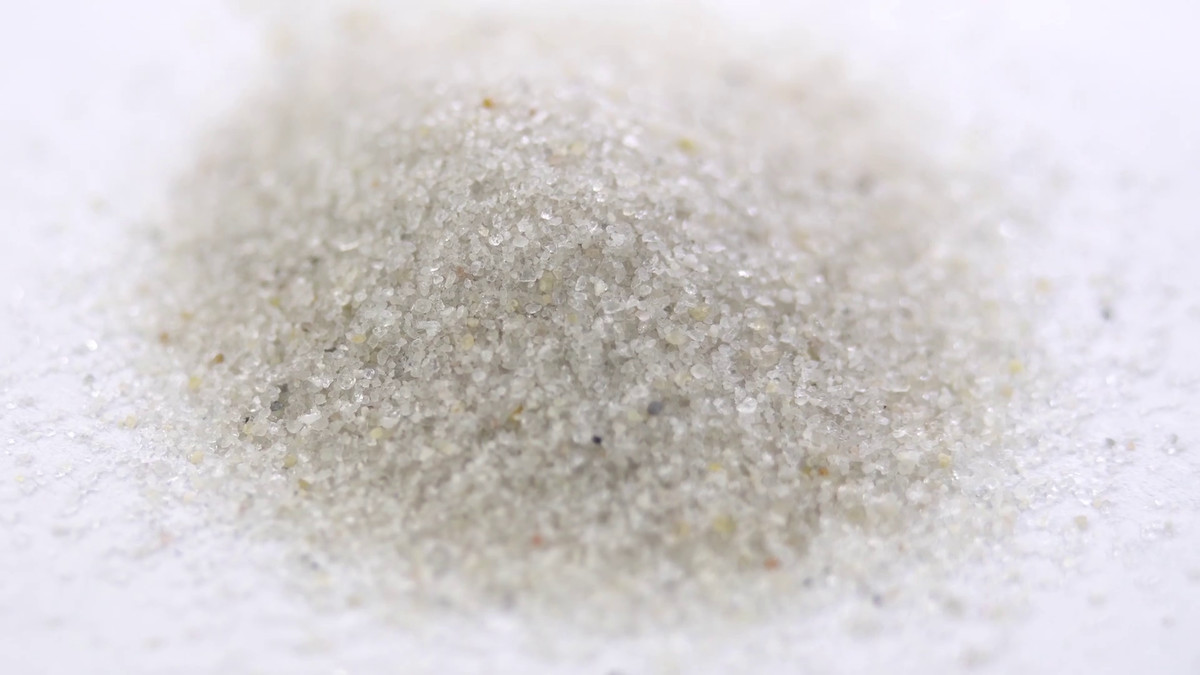
This is further refined into silicon dioxide with a purity of 99.9%.
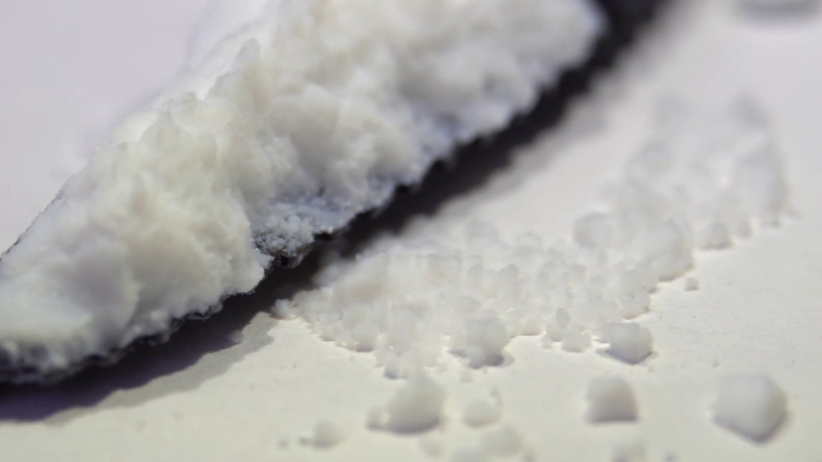
Furthermore, this silicon dioxide is refined into 99.9999999% polycrystalline silicon. The chemical formula is SiO 2 + 2C → Si + 2CO
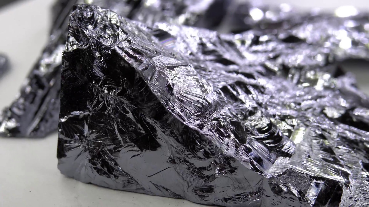
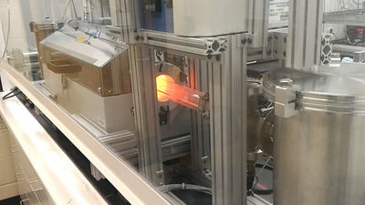
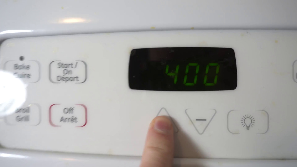
This polycrystalline silicon is melted at high temperature.
The temperature is 1698K (about 1425 ℃). Of course, it is a temperature that can not be put out with a kitchen stove for home use.
Immerse the seed single crystal silicon in the melted polycrystalline silicon and slowly pull it out while cooling it ...
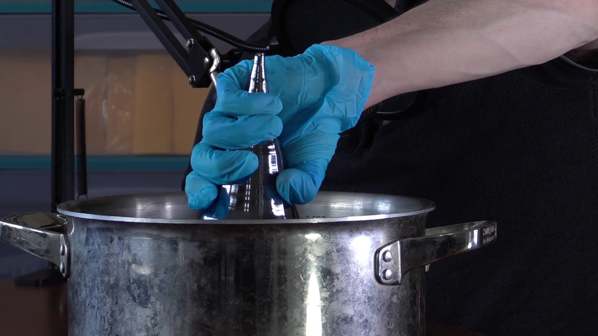
A huge silicon single crystal is formed. The method of immersing a small single crystal in molten silicon to grow and pull up an ultra-high purity single crystal is called the
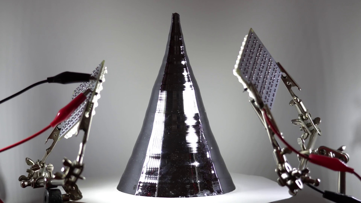
This silicon single crystal is sliced thinly.
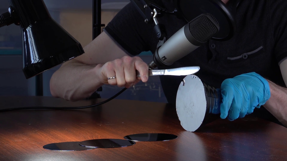
This silicon wafer is sliced and polished to a mirror surface. When boron is added to this silicon wafer,
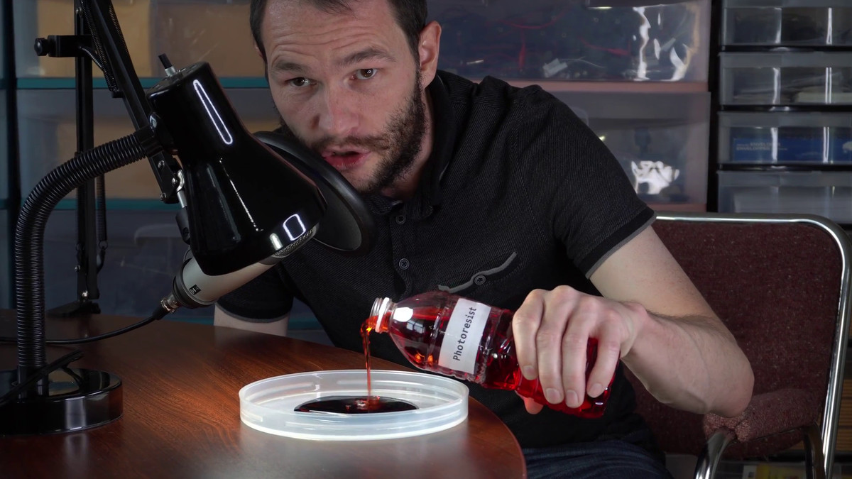
An oxide film is formed on the silicon wafer, and a photosensitive agent is applied on it.
Mr. Elder has a quartz mask pattern with a printed circuit pattern.
By irradiating ultraviolet rays through this mask pattern, the circuit pattern is printed on a thin film of photosensitive agent.
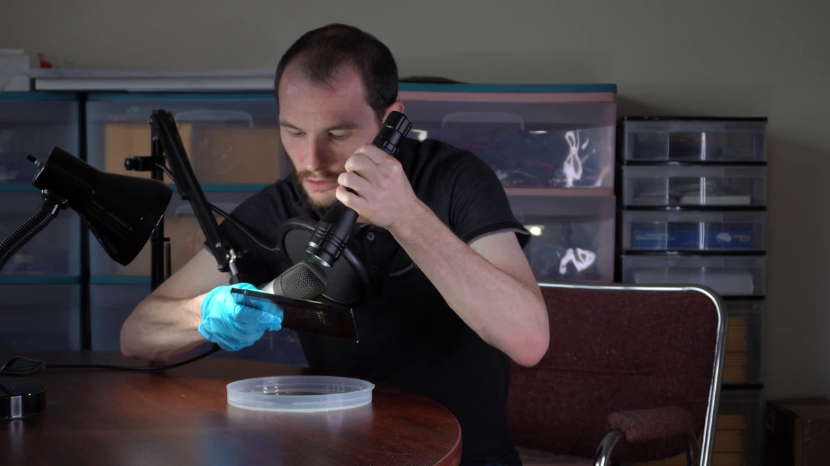
After baking, wash the wafer with a developer.
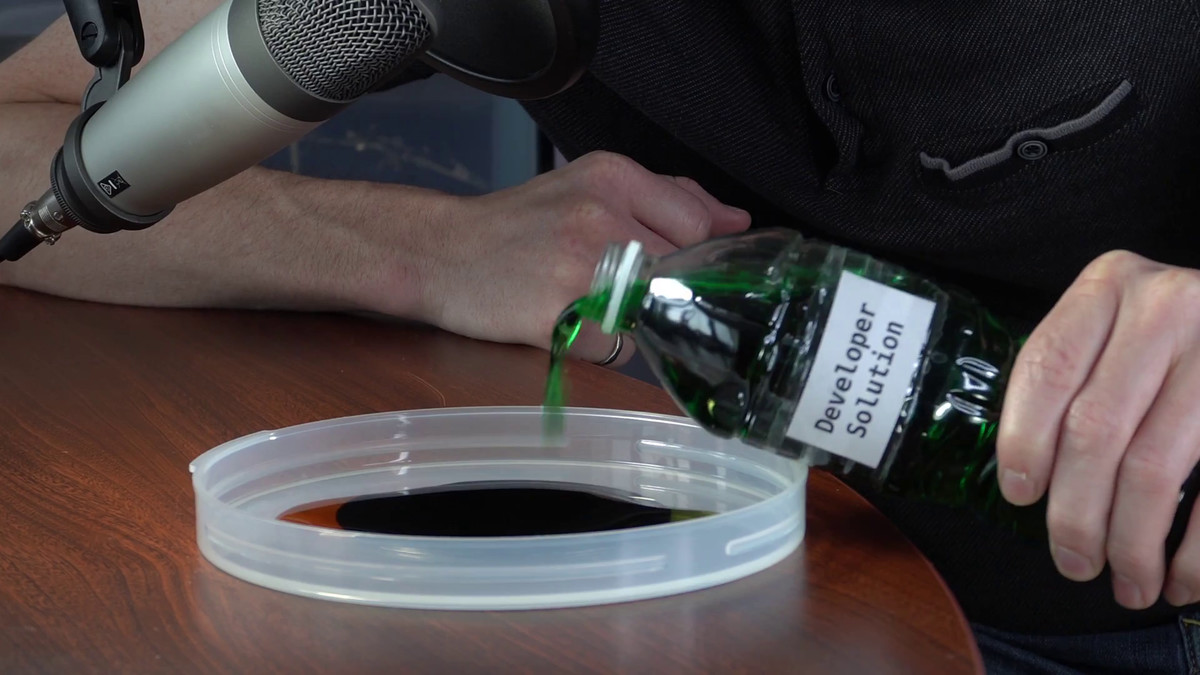
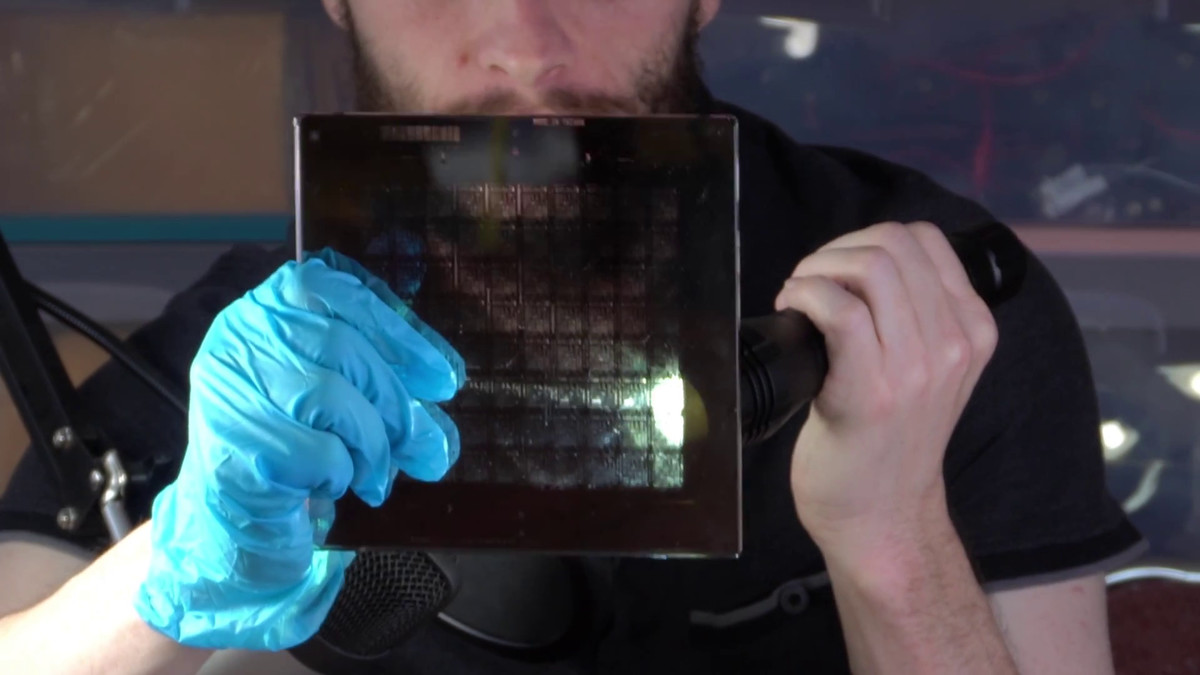
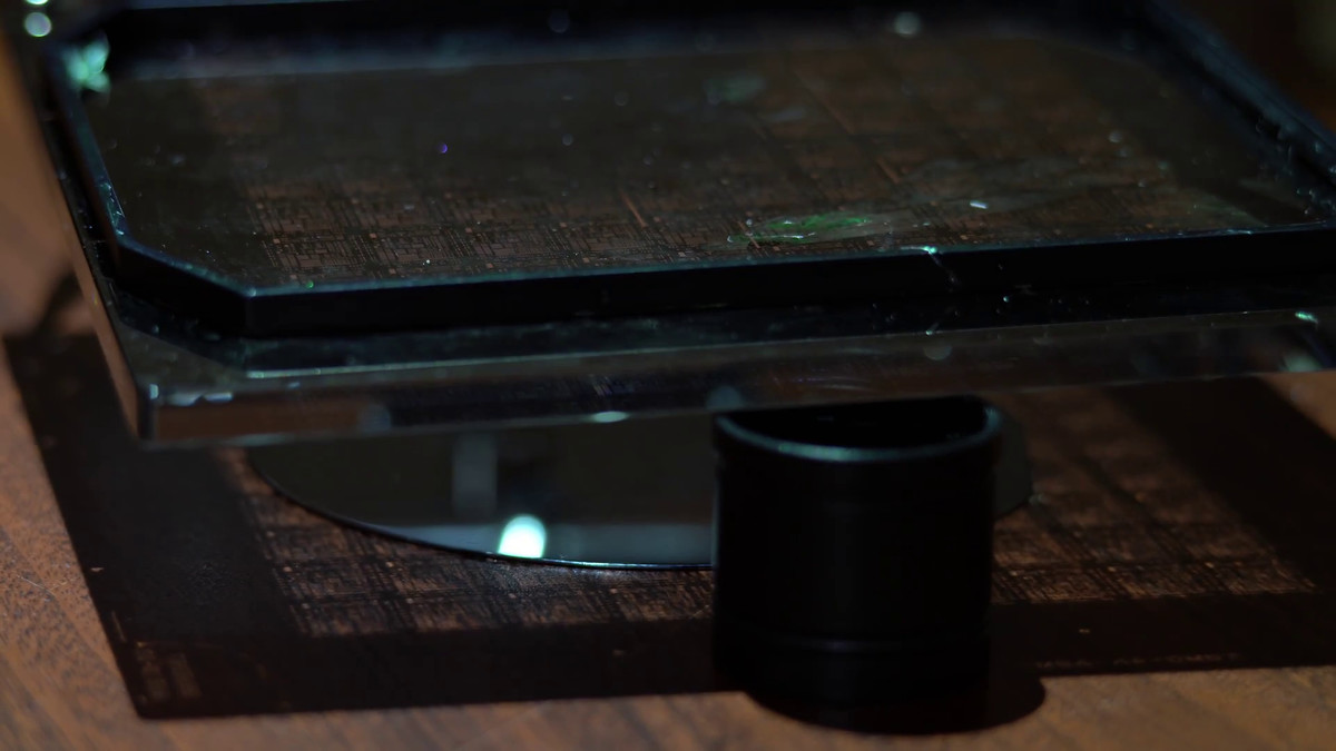
In addition, etching is performed using a corrosive agent. The photosensitive agent on the part of the mask pattern exposed to ultraviolet rays is removed with a developing solution. In other words, if the oxide film is exposed only in the circuit part and a corrosive agent is used here, the oxide film is also removed only in the circuit part and the silicon wafer is exposed.
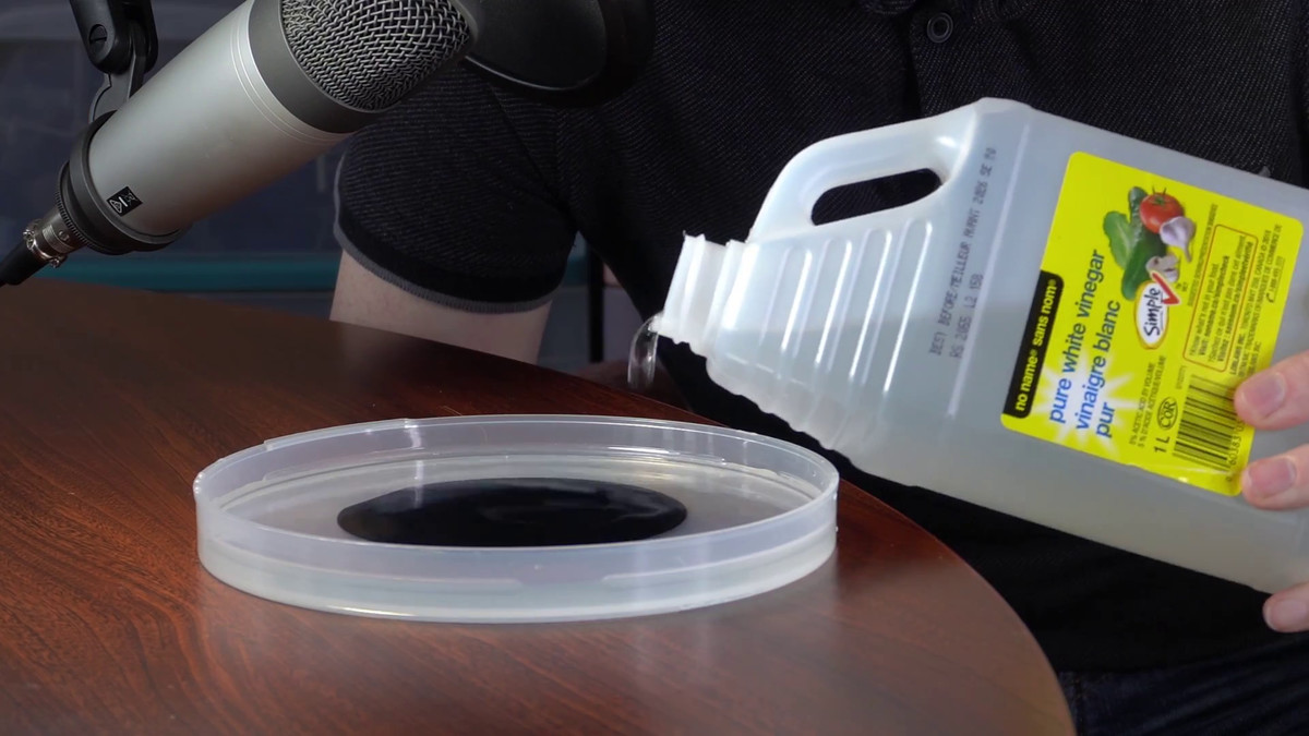
When you wash the wafer with pure water ...
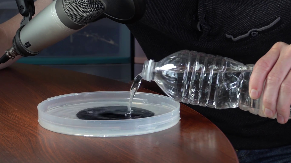
The circuit pattern can be seen on the surface of the silicon wafer as shown below.
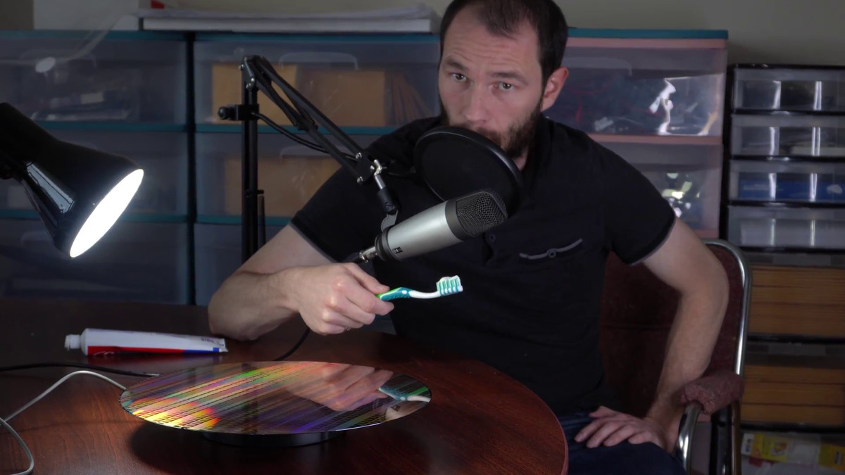
From here, various treatments and polishings are performed many times until silicon becomes a semiconductor with electrical characteristics.
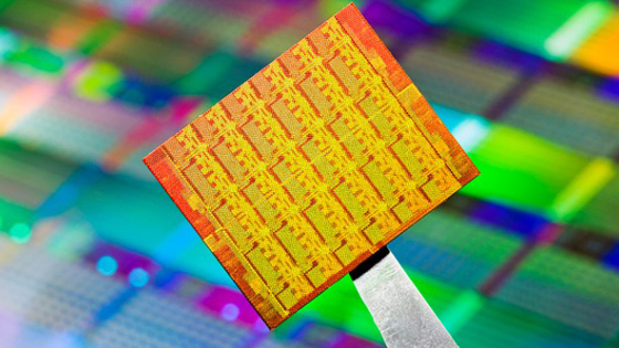
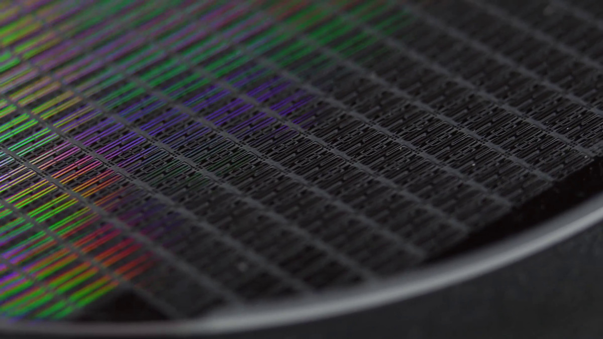
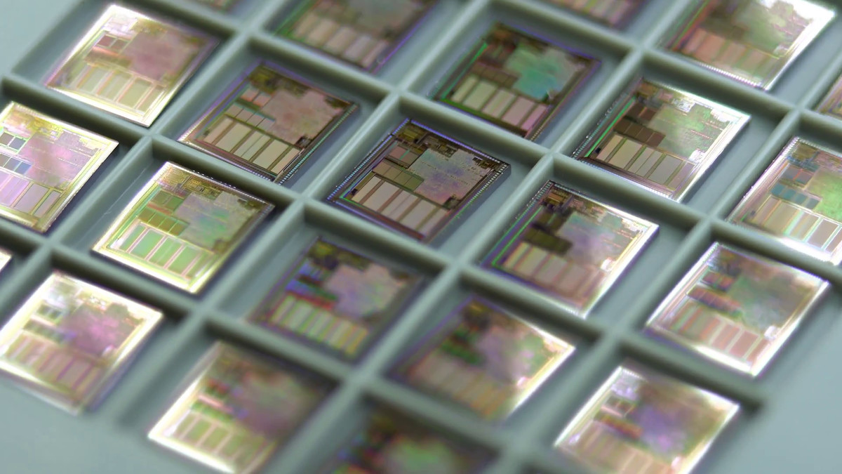
This completes the silicon wafer. The circuit of one chip is printed on one silicon wafer.
I will cut this silicon wafer into small pieces.
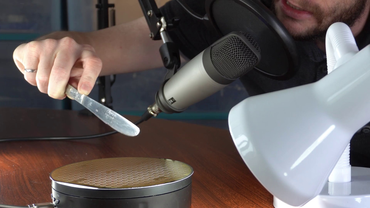
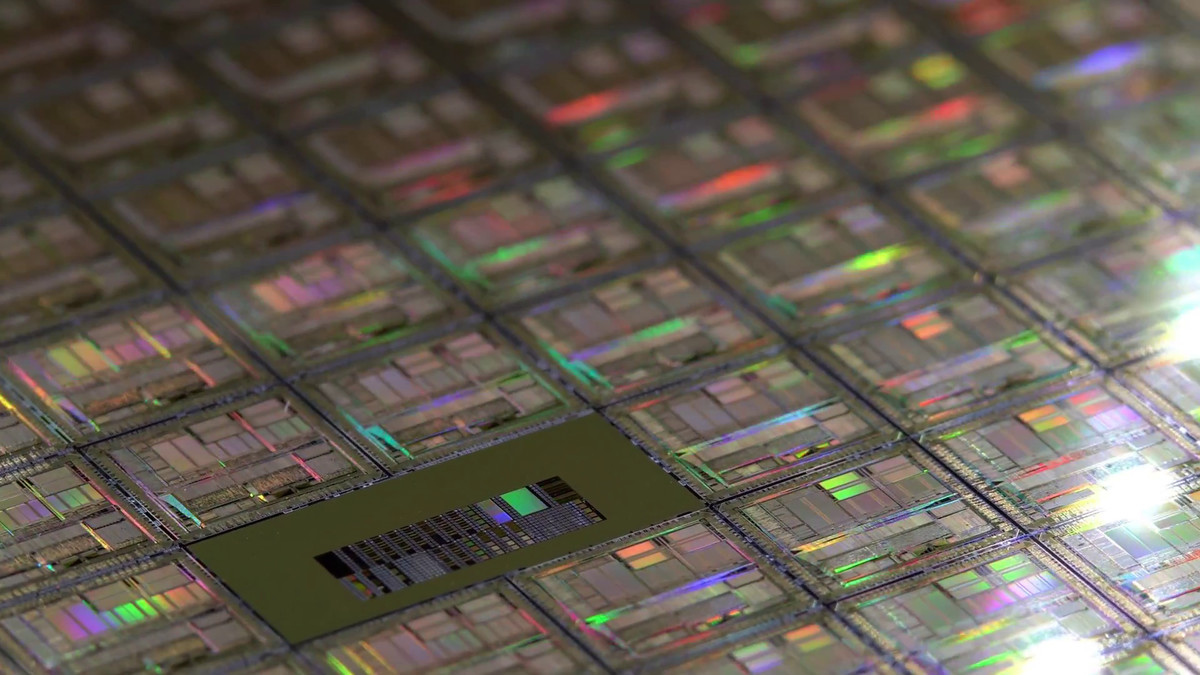
It looks like this when separated one by one. Good and defective products are sorted for each. The ratio of non-defective products obtained from this single wafer is called the 'yield rate'.
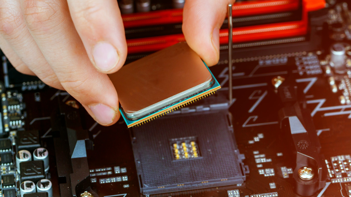
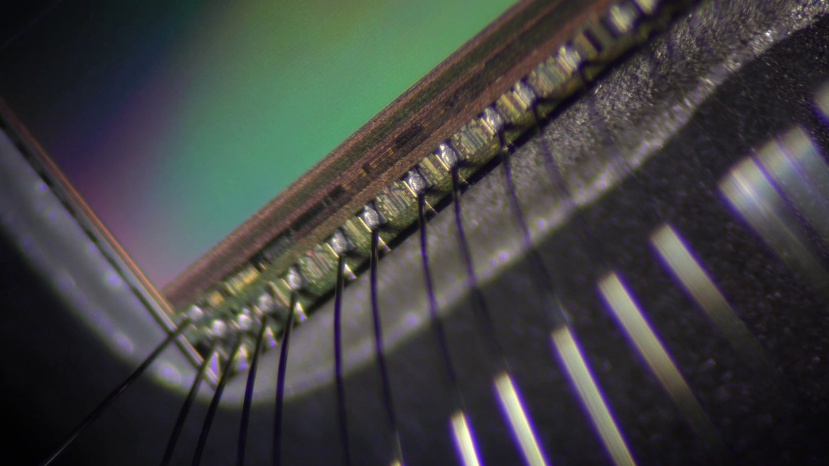
Manufactured chips are electrically connected to substrates and electrodes using thin conductors ranging from a dozen micrometers to hundreds of micrometers.
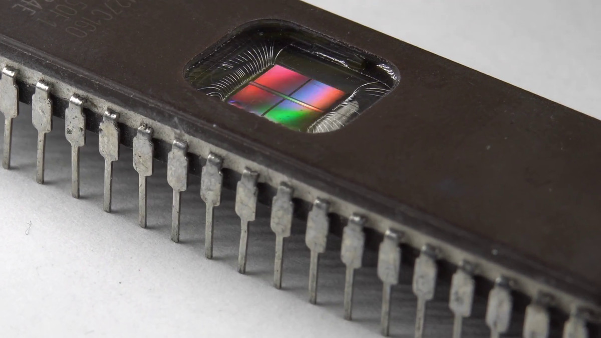
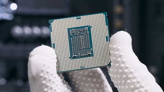
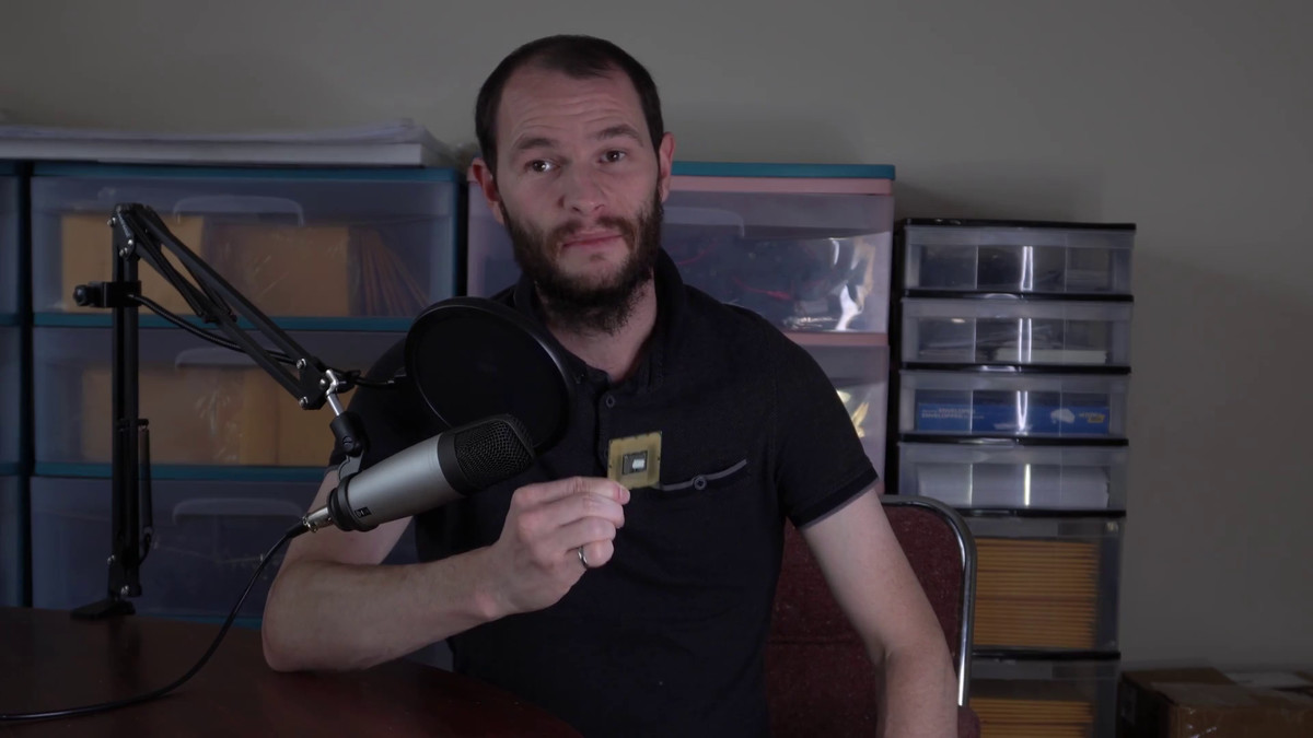
This chip is quite large, but the state-of-the-art CPUs used in PCs and servers are designed and manufactured in smaller sizes.
Of course, working on the movie is just a joke, so I'm not really making it. It is extremely difficult for individuals to make semiconductor chips from silicon, and nanometer units such as TSMC and Intel are impossible. However, according to Mr. Elder, even individuals can challenge if it is in the micrometer unit, for example, Mr. Sam Zeloof of YouTuber has published on YouTube how to make a semiconductor chip from silicon at home.
Upgraded Homemade Silicon Chips-YouTube
Related Posts: