TSMC is developing an advanced AI semiconductor packaging technology, which it internally calls 'quasi-EMIB,' and it may be similar to Intel's Embedded Multi-die Interconnect Bridge technology.
by
It has been reported that TSMC , the world's largest semiconductor contract manufacturer, is developing an advanced semiconductor packaging technology called 'quasi-EMIB' that mimics parts of Intel's EMIB, in response to the increasing number of orders for Intel's EMIB.
TSMC Develops AI Chip Packaging Tech to Counter Intel — The Information
https://www.theinformation.com/articles/tsmc-develops-ai-chip-packaging-tech-counter-intel
TSMC Concedes Intel's EMIB Packaging Is A Potent Contender, Starts Building 'Quasi-EMIB' As CoWoS Remains Choked Through 2026
https://wccftech.com/tsmc-concedes-intels-emib-packaging-is-a-potent-contender-starts-building-quasi-emib-as-cowos-remains-choked-through-2026/
TSMC is developing CoWoS as a 2.5D packaging technology, which will serve as the foundation for HPC and AI products. CoWoS-S, in particular, uses a large and expensive silicon interposer to connect the processor and high-bandwidth memory (HBM). It employs a full silicon interposer layer with a uniform grid of microbumps across the entire bottom surface of the die, which functions as the interconnection medium.
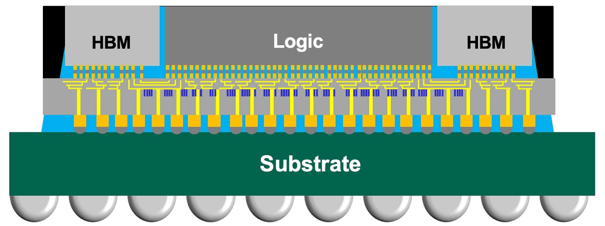
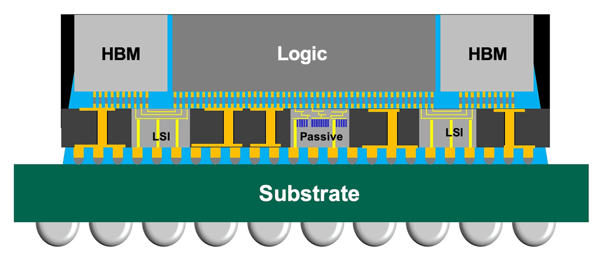
TSMC has revolutionized this approach with CoWoS-L, which completely eliminates the large, continuous silicon interposer layer and replaces it with a flexible, low-cost
In contrast, Intel's 2.5D packaging technology,
Instead of routing signals through huge, expensive silicon layers and RDLs that span the entire chip, EMIB acts as a localized connectivity path, placed only where two chips need to communicate with each other. Technology media outlet Wccftech wrote about Intel's EMIB: 'To understand the efficiency of Intel's approach, consider the fact that EMIB uses no intermediate layers at all. Chiplets are placed directly on the organic substrate and connected to each other via embedded bridges by a single connectivity process.'
In contrast, TSMC's CoWoS-L employs a completely independent RDL interposer. A local silicon interconnect (LSI) bridge is embedded within this intermediate carrier, and the combined structure of the RDL and bridge is fabricated on a conventional circular silicon wafer and bonded to the organic substrate beneath it. Therefore, two different assembly and bonding processes are required.
Furthermore, Intel's next-generation technology, 'EMIB-T,' employs TSVs (Through-Silicon Via) that directly penetrate embedded silicon bridges. This allows power and high-speed signals to flow directly from the bottom of the chip package through the bridge to the processor and memory above, enabling 3D stacking.
According to The Information, TSMC is developing a new 2.5D packaging technology, internally referred to as 'quasi-EMIB,' which is based on Intel's EMIB. 'Quasi-EMIB' is being developed in collaboration with KINSUS , a leading manufacturer of semiconductor packaging substrates. While details are unclear at the time of writing, it is speculated that TSMC is completely eliminating the redistribution layer and instead employing silicon bridges similar to EMIB.
Related Posts:


in Hardware, Posted by logu_ii