What exactly is the 'RDNA 3 architecture' adopted for AMD's GPU 'RX 7900 series'?
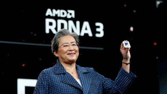
On November 3, 2022, AMD revealed the details of the next-generation GPU architecture '
AMD RDNA 3 GPU Architecture Deep Dive: The Ryzen Moment for GPUs | Tom's Hardware
https://www.tomshardware.com/news/amd-rdna-3-gpu-architecture-deep-dive-the-ryzen-moment-for-gpus
The GPU 'Navi 31' made using the RDNA 3 architecture is a GPU die (GCD) manufactured by the 5nm process and a cache memory (MCD) manufactured by the 6nm process are combined into one package by adopting a chiplet. I'm here. This improves memory bandwidth to a maximum of 5.3 TB / s and processing performance to 61 TFLOPS. The performance per power consumption has increased by 54% compared to the previous generation 'RDNA 2', and the performance has been renewed in various aspects.
The chiplet is a design that AMD has adopted since ' Zen 2 ' of the CPU microarchitecture, and the CPU after Zen 2 uses a die (IOD) equipped with an input/output circuit to connect to the system memory, PCIe interface and We have made sure that all features are available, including USB ports, Zen 4 graphics and video capabilities. In addition, AMD uses a design called Infinity Fabric to connect the Core Compute Die (CCD), which consists of CPU cores and caches, to the IOD.
Mr. Walton explained that the design point is that most of what runs on the CPU core fits in the various caches of L1, L2, and L3. Modern CPUs up to Zen 4 have only two 64-bit memory channels for system RAM.
The CCD is small, and the IOD is about 125 square millimeters to 416 square millimeters. Most recently, the Zen 4-equipped 'Ryzen 7000 series' IOD features an IOD of just 122 square millimeters with one or two 70-square millimeter CCDs manufactured on TSMC's 5nm process (N5). It is said that the 4th generation EPYC has a relatively large IOD of 396 square millimeters while adopting the same CCD.
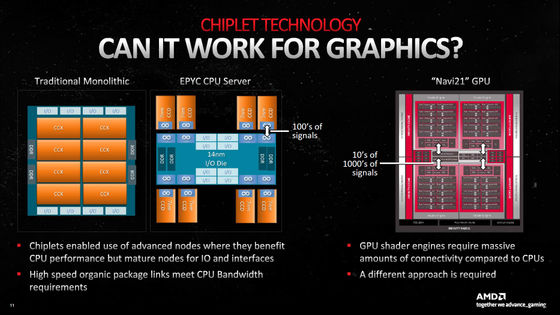
However, the requirements for these CPUs and the requirements for GPUs are very different. GPUs require large caches and a large amount of memory bandwidth, and simply compared to CPUs, even the huge '
``In other words, AMD had to take a different approach than the CPU to make the GPU chiplet work effectively,'' Walton said. The solution AMD came up with was to put the memory controller and cache on multiple smaller dies, almost the opposite of the CPU chiplet, and put the main compute function on the central GCD chiplet.
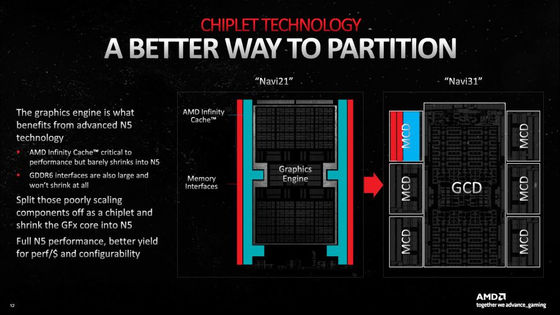
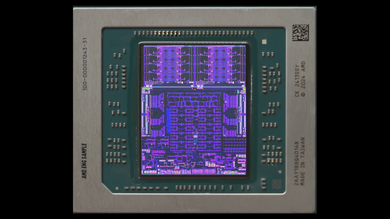
GCD includes all Compute Units (CU: the smallest unit of computing resources, including cores, schedulers, register files, instruction caches, texture/L1 caches, extractor mapping units, etc.), video codec hardware, display interfaces, Core features such as PCIe connectivity are included. The Navi 31's GCD has up to 96 CUs, which is where the general graphics processing takes place, as well as the Infinity Fabric on the top and bottom edges, which connects to the MCD from there.
GCD uses TSMC's N5 node and has 45.7 billion transistors on a 300 square millimeter die. On the other hand, MCD is manufactured at TSMC's 6 nm process (N6) node, with 2.05 billion transistors each on a chip of only 37 square millimeters. Cache and external interfaces have an average of 152.3 million transistors per square millimeter for GCDs, while MCDs average 55.4 million transistors per square millimeter.
``One potential concern with the GPU chiplet approach is how much power the components around the Infinity Fabric require,'' Walton said. For example, the board called interposer used for Zen CPU consumes considerable power when enlarged to GPU scale. That's why AMD worked on improving the interface with Navi 31.
The result is a design called 'High Performance Fanout Interconnect', which is incorporated in the Navi 31 part on the right side of the image below. On the left is the organic substrate used in the Zen CPU, and both in the image are displayed in almost the same size ratio as in reality. The left side has 25 wires, but the right side has evolved into an ultra-high density design with 50 wires in a smaller area.
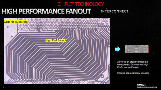
As a result, all the components around the Infinity Fanout together achieve an effective bandwidth of 3.5 TB / s, while operating at less than 5% of the power consumption of the entire GPU.
In addition to doubling the throughput of floating-point operations, RDNA 3 also doubles the throughput of matrix (AI), resulting in an overall 2.7-fold increase in matrix operation speed. In addition to the cache and system, all interfaces between parts have been upgraded, for example, the L0 cache has increased to 32KB, which is double that of RDNA 2, the L1 cache has also doubled to 256KB, and the L2 cache has increased to 6MB, which is 1.5 times. . The link between the main processing unit and the L1 cache has increased by 1.5 times, resulting in a throughput of 6144 bytes per clock, and the link between the L1 cache and the L2 cache is also 1.5 times wider.
Although the RX 7900 series that uses such RDNA 3 is not as good as NVIDIA's RTX 4090, it may be able to compete with the RTX 4080. 'A simple calculation shows that 12,288 shaders of 32-bit floating point run at 2.5 GHz, while NVIDIA's 16,384 shaders run at 2.52 GHz, so NVIDIA's 61 TFLOPS and AMD's 83 TFLOPS, clearly superior. You can see that you can stand,' Walton pointed out. In addition, the memory bandwidth seems to be at least pretty close, and he said the difference probably shouldn't matter too much, but he said he won't know until AMD's RX 7900 series comes out anyway.
Walton said, ``The good news for those who aren't interested in $900+ graphics cards is that 2023 will see the RTX 4070 and lower Ada Lovelace parts, and AMD's RX 7800, 7700, and 7600 series. From what we've seen and heard so far, the future RTX 4070 and RX 7800 should perform similarly to their predecessors, the RTX 3090 and RX 6950 XT, at a lower price point. It will likely be provided,' he said.
Related Posts:
in Hardware, Posted by log1p_kr
