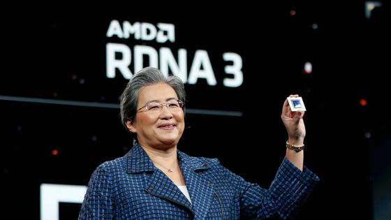
What is so special about the AMD Ryzen AI MAX series, a high-performance mobile APU that is said to 'contain the DNA of the Zen 6 generation'?
Semiconductor manufacturer AMD announced
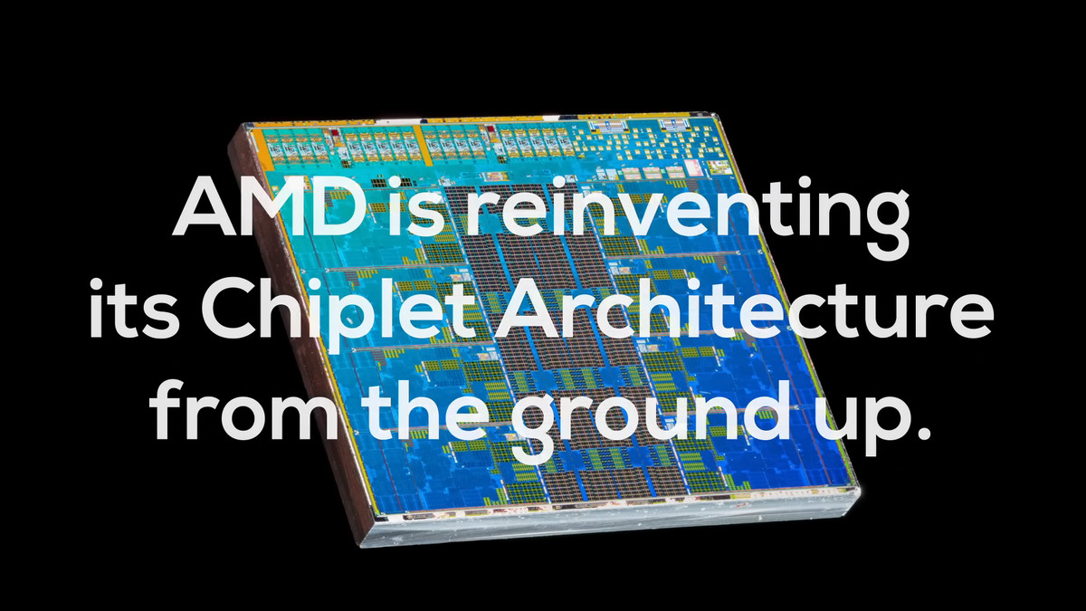
How AMD is re-thinking Chiplet Design - YouTube
High Yield claims that AMD is rebuilding its chiplet architecture with new layout, silicon, and packaging, and that the Ryzen AI MAX series offers a glimpse of 'ZEN 6 DNA.'
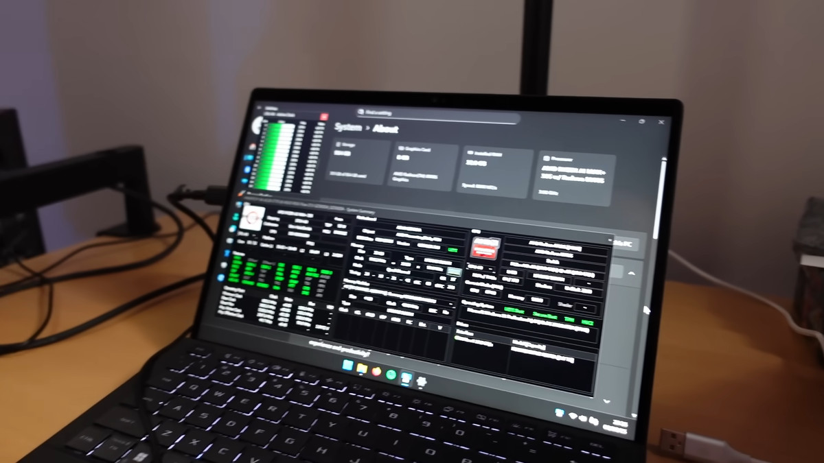
The Ryzen AI MAX series has already been shipped to the market, and is also installed in the ASUS notebook PC '
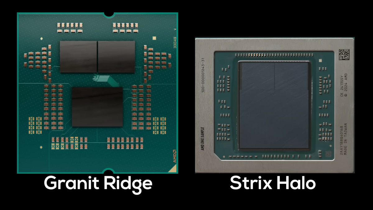
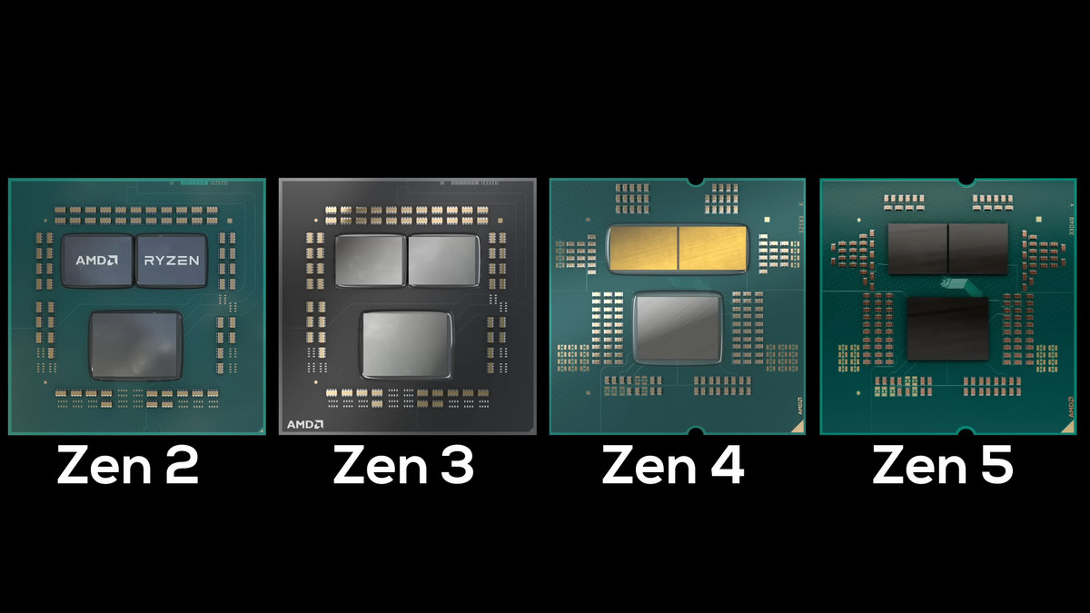
AMD has completely redesigned its chiplet design since Zen 2, adopting new silicon, packaging, and layout. The first to adopt this next-generation design is the mobile APU Ryzen AI MAX series (Strix Halo).
AMD's
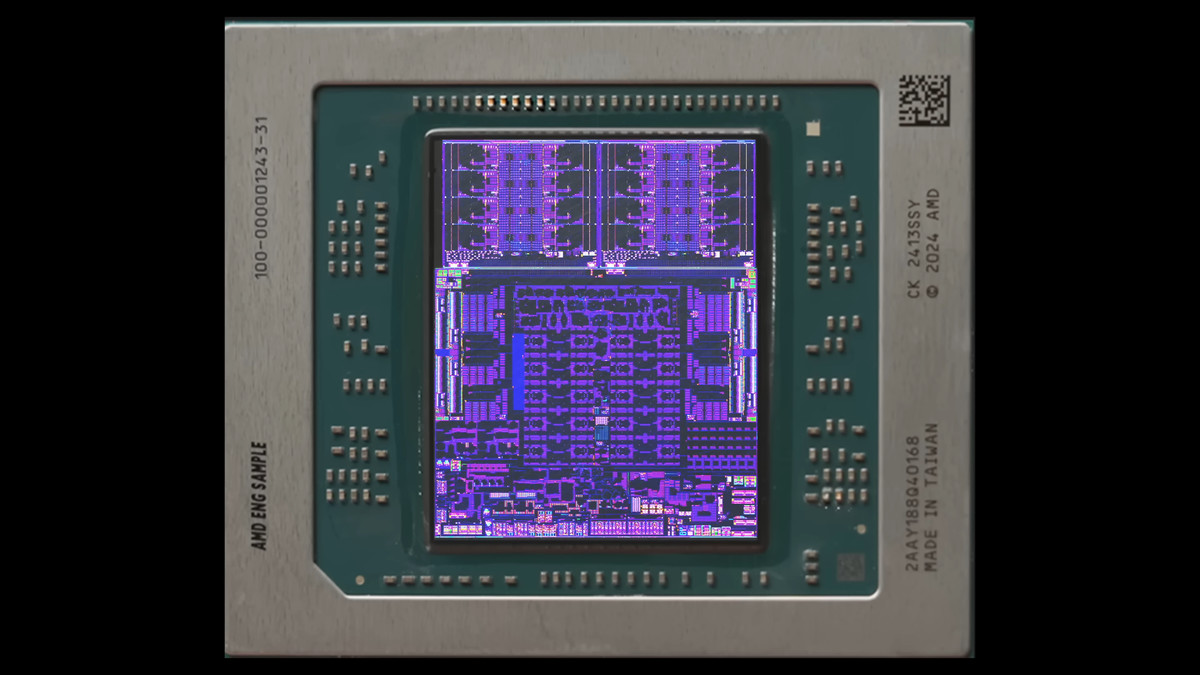
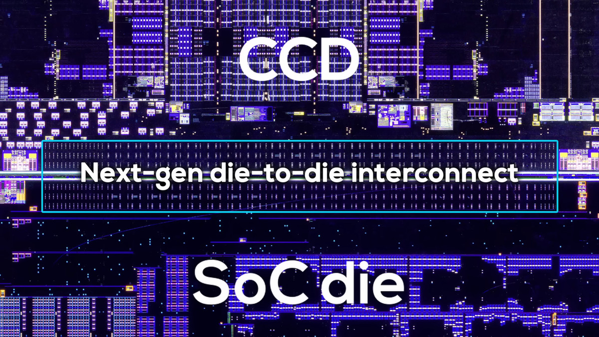
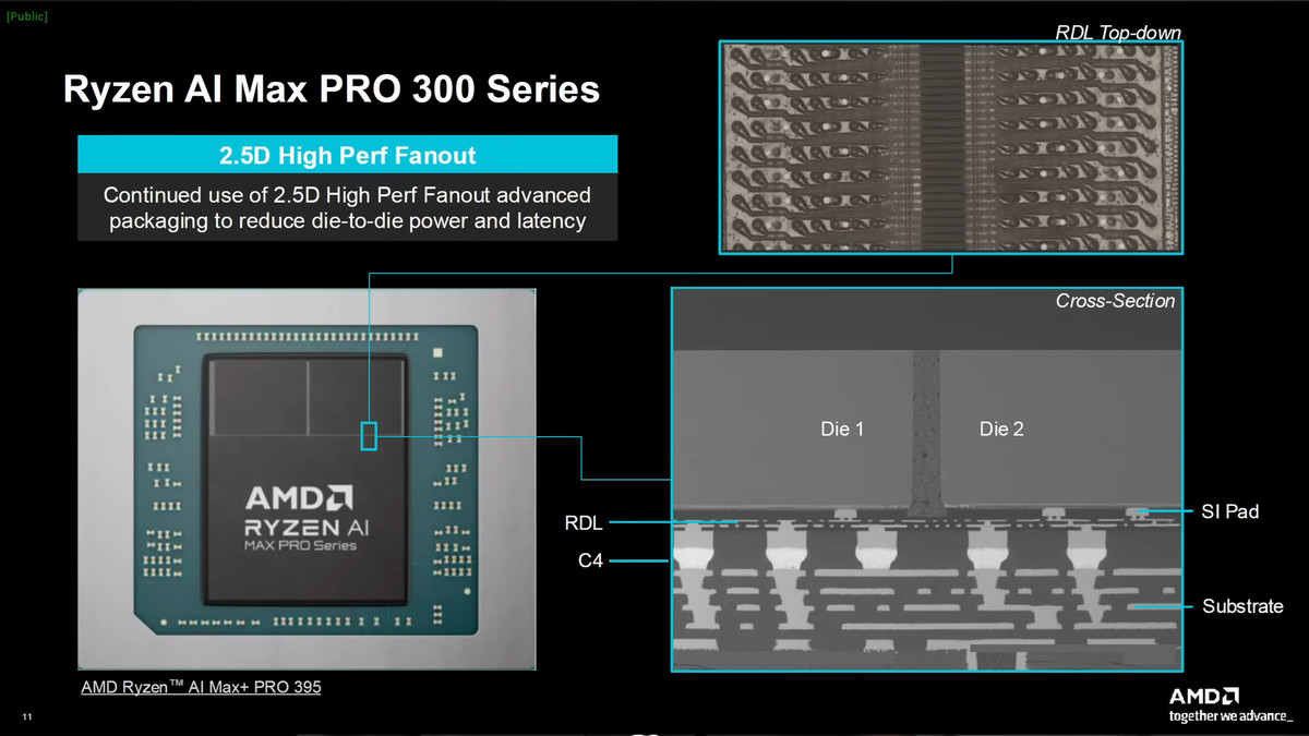
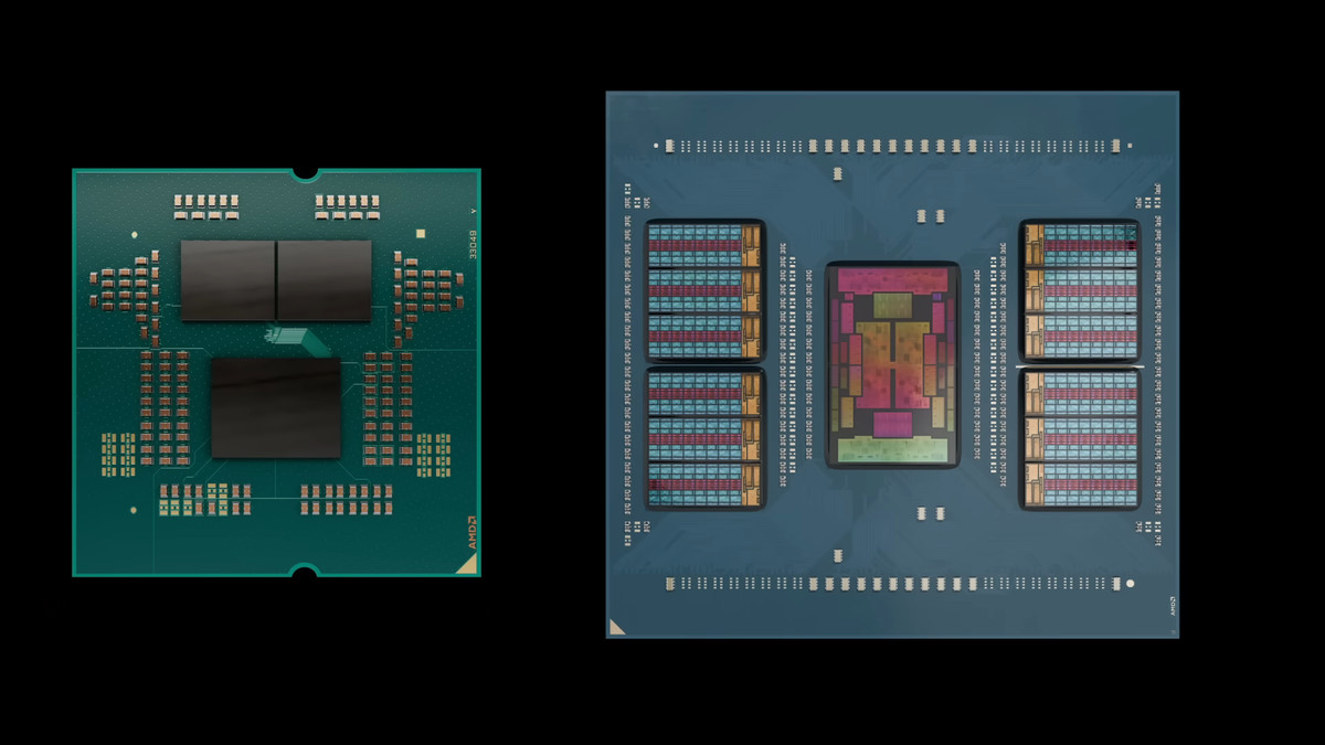
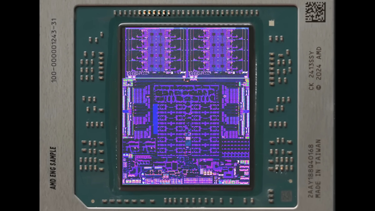
Unlike the traditional AMD chiplet design seen since Zen 2, the Strix Halo looks more like Intel's tile-based design. It consists of two CPU chiplets (CCDs) fabricated on TSMC's N4P process and a massive SoC die measuring approximately 307mm² .
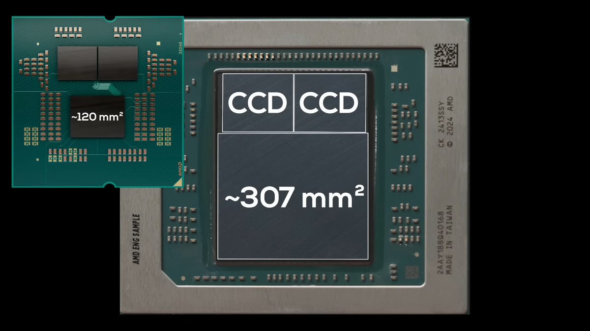
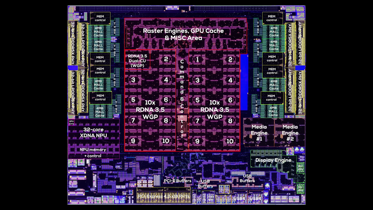
The SoC die features eight 32-bit LPDDR5X memory modules, four on each side of the chip, providing a 256-bit high-bandwidth interface and a 32MB L3 cache. This provides approximately twice the memory bandwidth of competing APUs. The center of the chip houses a large integrated GPU with 40 RDNA 3.5 compute units (CUs), comparable in performance to the GeForce RTX 4060 and 4070 mobile versions. The left side of the SoC die also houses a 32-core XDNA NPU based on Xilinx technology. The right side houses the media engine and display engine, while the bottom side houses 16 lanes of PCI-Express 4.0, USB 2.0, USB 3.0, and USB 4.
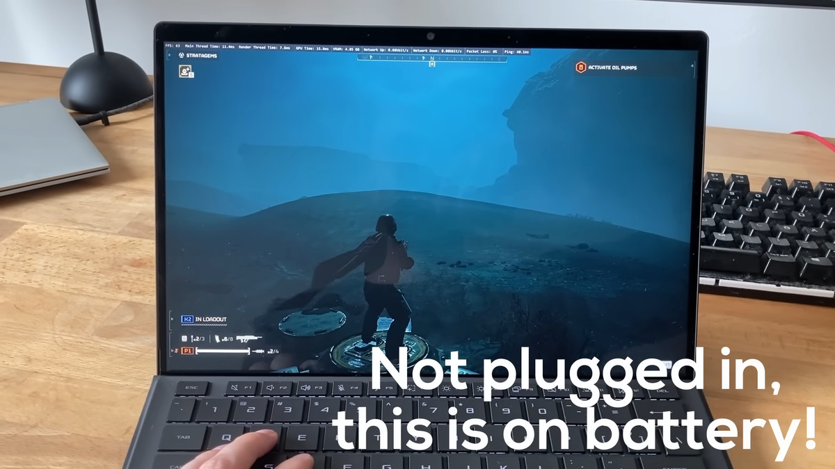
High Yield actually played the game '
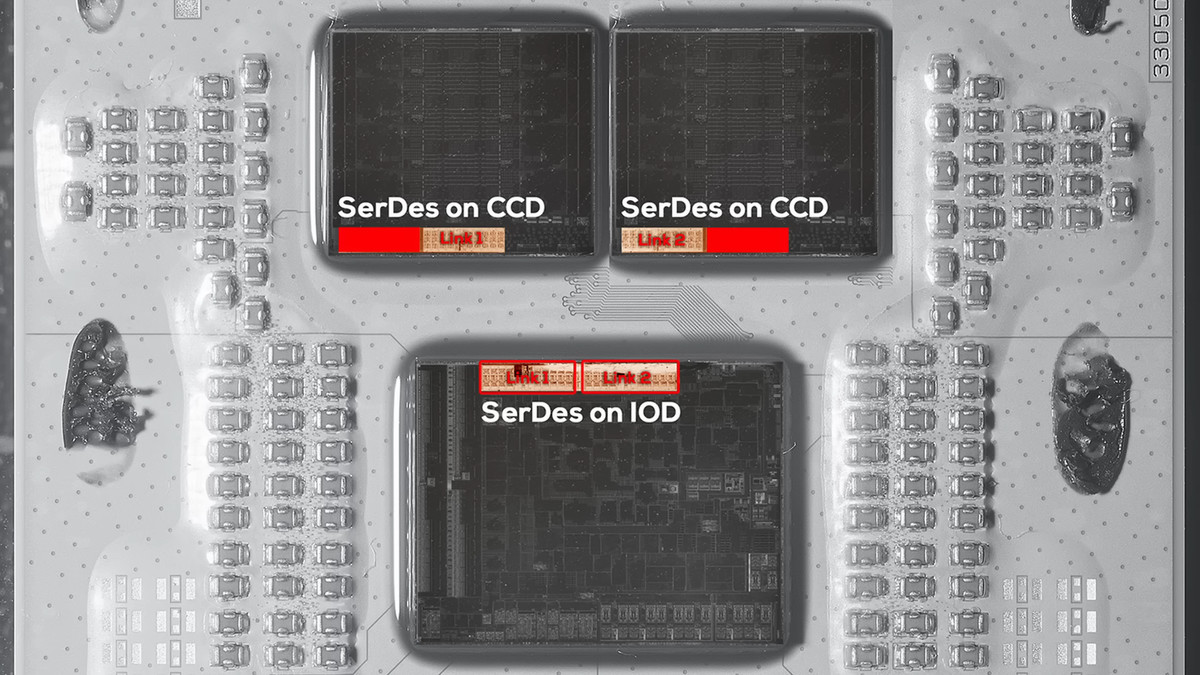
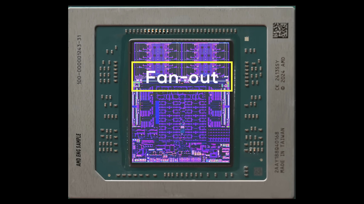
The rectangular area visible at the top of the SoC die is AMD's next-generation die-to-die interconnect, which High Yield says 'is the DNA of ZEN 6.'
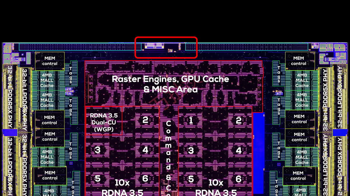
Looking at the die photo, we can see that this rectangular area at the top of the SoC die corresponds to two CCDs.

Looking at this next-gen inter-die interconnect, unlike the Zen 5 SerDes, it is made up of many rows of small interconnects.
AMD's 'Infinity Fabric on Package' used in Zen 2 through Zen 5 is a serial interconnect using this SerDes, which is based on the PCI Express design and allows communication between chiplets.
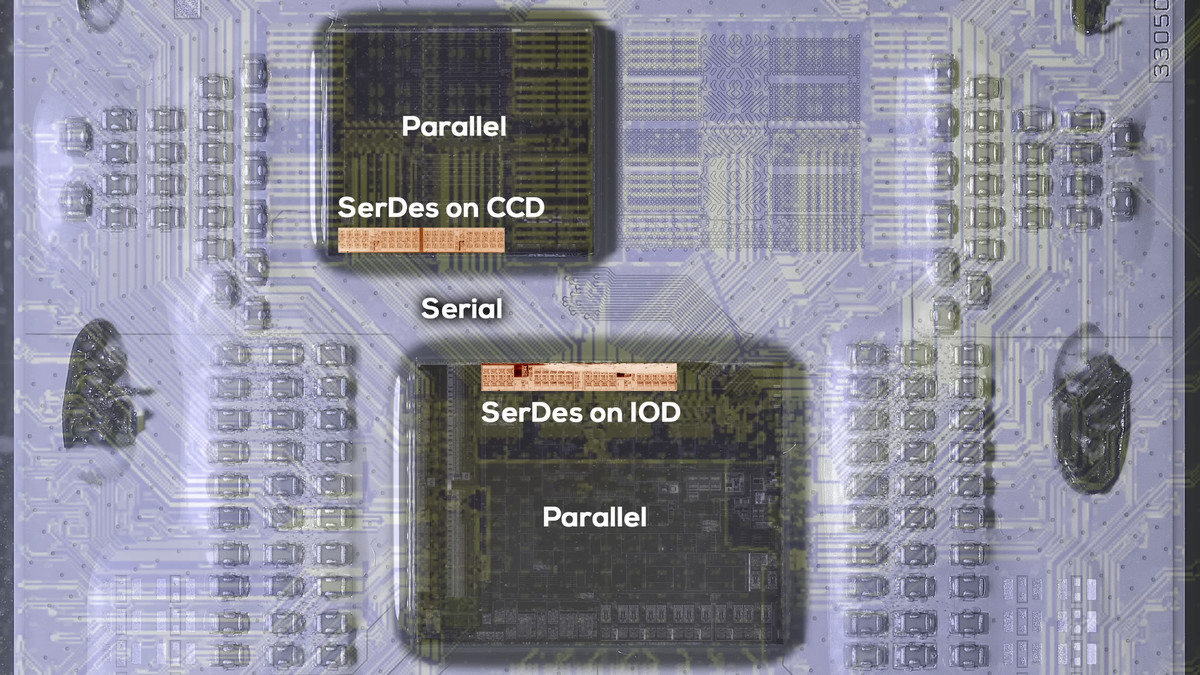
To put it in perspective, the SerDes and wiring are the physical layer, like a 'highway,' and the Infinity Fabric protocol that determines how data is transferred is the 'car' that runs on top of it.

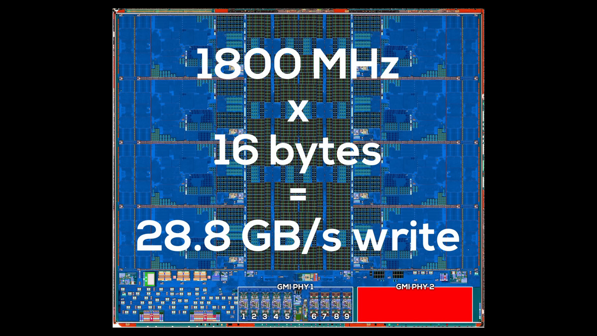
The Ryzen CPU's Infinity Fabric consists of two independent links called Global Memory Interconnect (GMI), each consisting of an 8-bit wide serial interconnect and one parity bit, for a total of nine logic blocks.
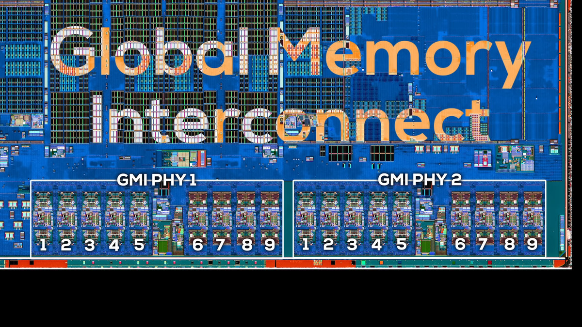
Consumer Ryzen CPUs use a GMI-narrow implementation that uses only one link, so one of the two links on the CCD is always unused, while server EPYC CPUs use GMI-wide, which uses both links.
Because Ryzen CPUs use GMI-narrow, a single CCD cannot fully utilize the memory bandwidth. A single CCD configuration results in worse memory bandwidth than a dual CCD configuration.
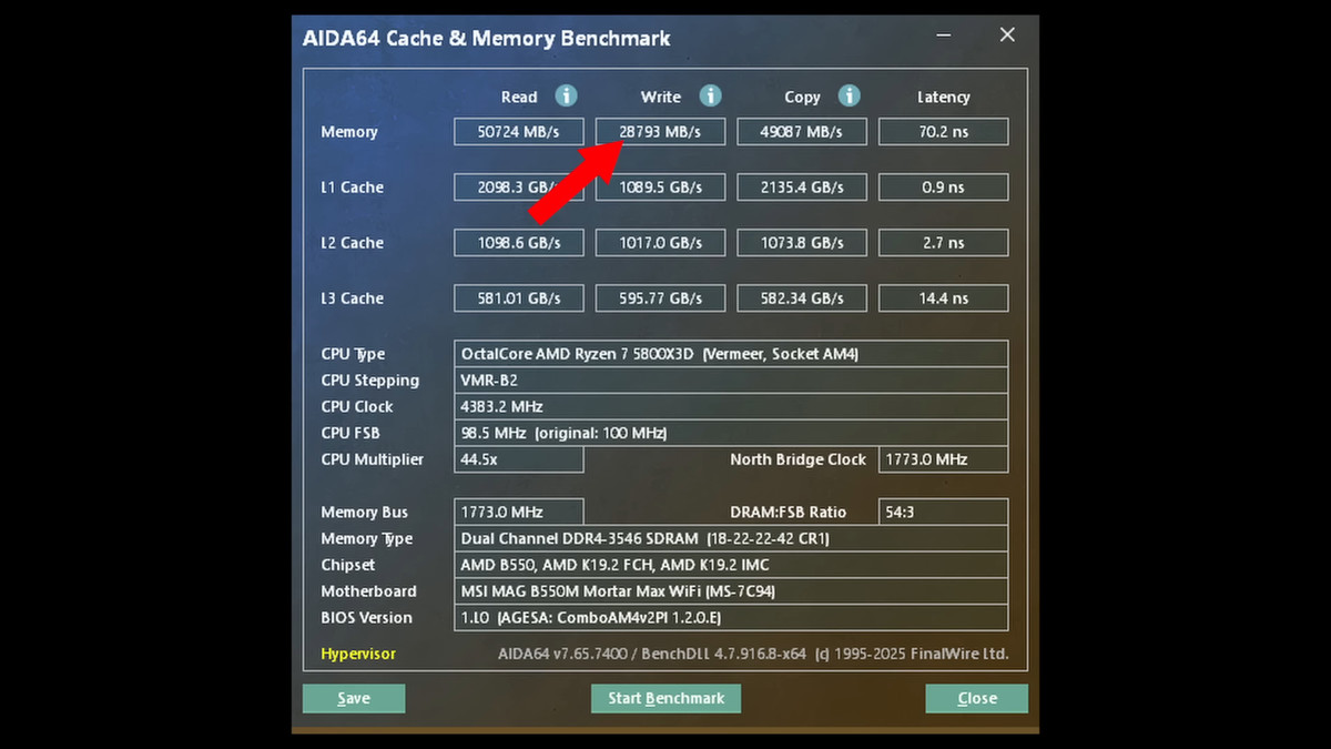
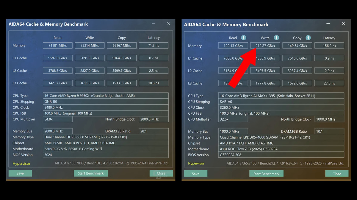
Using 8-bit GMI-narrow and an Infinity Fabric clock speed of 1800MHz, equivalent to DDR4-3600, the theoretical maximum bandwidth is 57.6GB/s read and 28.8GB/s write.
This is also supported by actual measurements.
SerDes is a combination of digital and analog systems, making it very difficult to shrink in size even at smaller process nodes, while the many rows of tiny interconnects found in Strix Halo CCDs cannot be SerDes due to their size and number.
According to High Yield, AMD is switching to a new interconnect method called 'fan-out interconnect.'
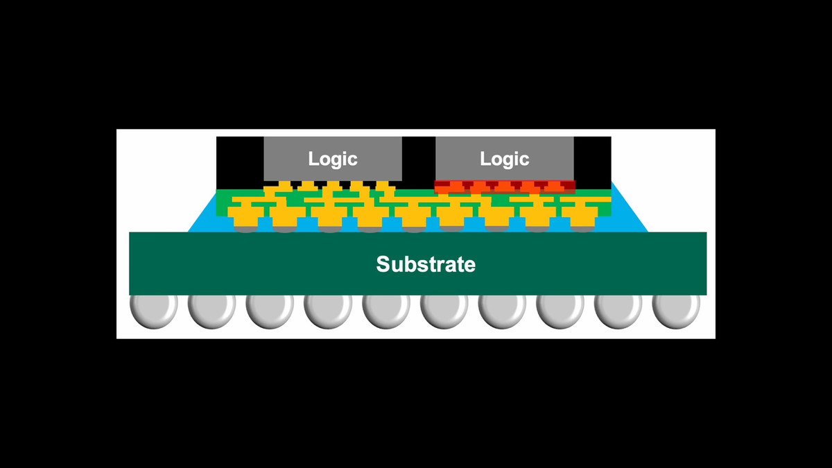
Fan-out interconnect is based on the simple concept of simply using wires directly from one chip to another, without going through a SerDes, to connect chips. It uses as many wires as possible to maximize parallel rather than serial connections, and employs a structure in which the wires fan out across the die boundaries.
However, in modern fan-out interconnects, the number of wires cannot be accommodated simply by spanning a single plane, so wiring is spread across multiple layers, requiring structures to support this complex multi-layer wiring system.
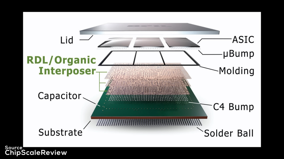
High Yield noted that the packaging technology AMD is using is almost certainly TSMC's 'InFO_oS (Integrated Fan-out on Substrate)' technology, where 'on Substrate' refers to fan-out technology integrated on the substrate.

Unlike TSMC's CoWoS and Intel's Foveros, InFO_oS does not use a silicon
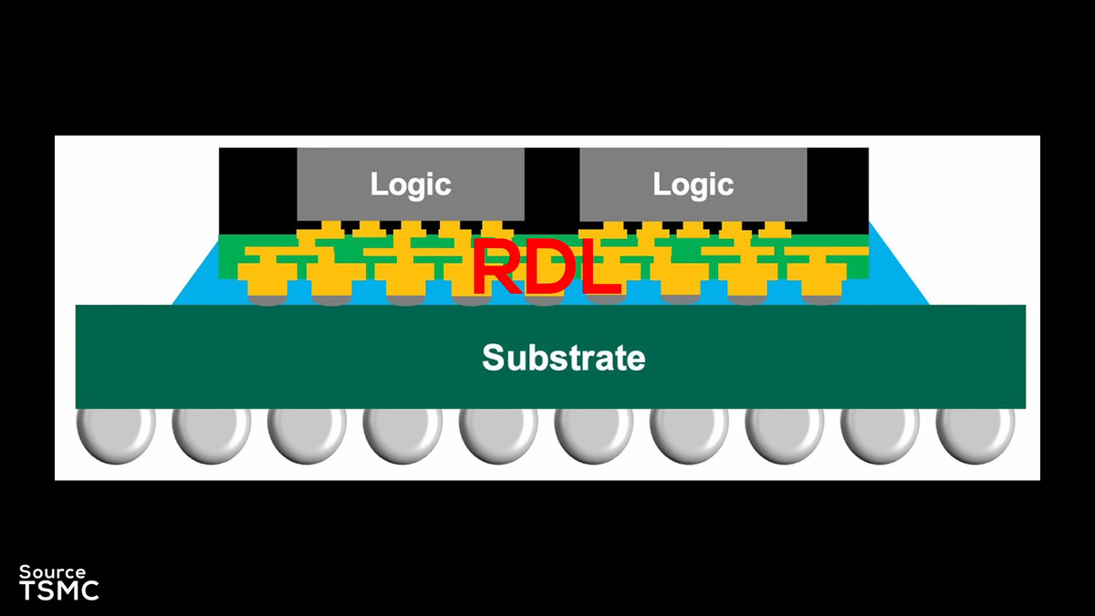
The RDL interposer consists of a layer of copper that carries the electrical signals and a layer of polymer dielectric material that insulates the signals from each other.
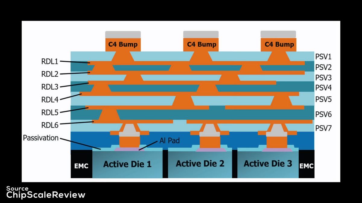
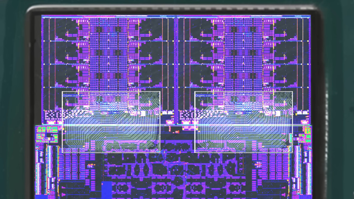
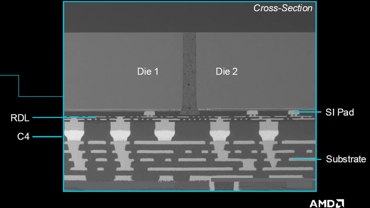
In Strix Halo, the SoC die and two CCDs sit on top of this RDL interposer, which routes hundreds of tiny interconnects between the CCDs and the SoC die.
A cross-section of the package reveals an RDL interposer sandwiched between the bottom substrate and the connection terminals (C4). The chiplets connect to the RDL interposer. The fan-out interconnect traces are much smaller than those in the substrate, and this miniaturization allows for high-density interconnects. This allows AMD to continue the CCD's internal data fabric directly onto the SoC die without signal conversion, eliminating the need for SerDes.
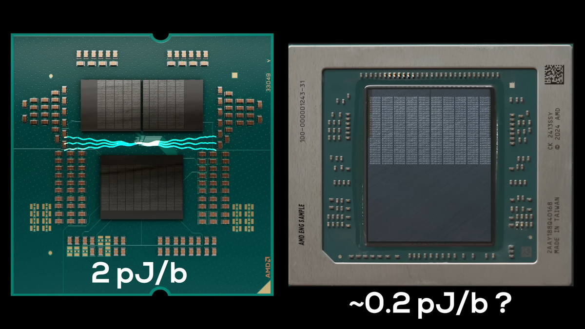
The biggest advantage of fan-out interconnect is the dramatic improvement in energy efficiency of data transfer and the elimination of latency due to the elimination of SerDes processing time. While the Zen 2 generation Infinity Fabric on Package consumed approximately 2 picojoules per bit, fan-out interconnect consumes only 0.2 picojoules, significantly reducing the energy required for data transfer.
Fan-out interconnects also provide higher bandwidth, similar to SerDes-based designs operating at higher frequencies. The Ryzen AI Max series also exhibits higher read, copy, and write bandwidth compared to the Ryzen 9 9950X, which uses the Zen 5 architecture, confirming improved interconnect bandwidth.
However, fan-out interconnect requires RDL interposers and advanced packaging techniques to create the fine interconnects, making it more complex and expensive to implement than traditional Infinity Fabric on Package solutions.
Additionally, while traditional SerDes-based Infinity Fabric allows chiplets to be connected over long distances, the new fan-out approach requires chiplets to be placed closely together, making the edge of the chip a limited resource.
Additionally, the new RDL interposer technology could have a significant impact on AMD's
SerDes-based interconnects are destined to become obsolete sooner or later, and fan-out technology is the perfect replacement. High Yield argued that the transition to fan-out technology is inevitable because the benefits, especially in energy efficiency and reduced latency in laptops and servers, outweigh the increased packaging complexity and cost.
Related Posts: