AMD Chief Technology Officer talks about 'Zen 3 architecture' adopted by 4th generation Ryzen CPU
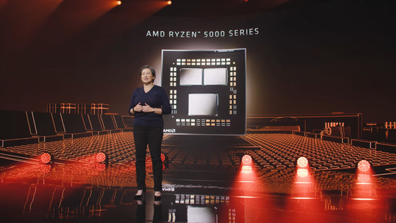
AMD's ' Ryzen 5000 ' series of CPUs is a Zen 3 architecture desktop CPU that uses TSMC's 7nm process and will be available on November 5, 2020. Technology media AnandTech interviews AMD's Chief Technology Officer (CTO) Mark Papermaster about the Zen 3 architecture.
AMD Zen 3: An AnandTech Interview with CTO Mark Papermaster
https://www.anandtech.com/show/16176/amd-zen-3-an-anandtech-interview-with-cto-mark-papermaster
Q: Q:
When interviewing Lisa Su, President and CEO of Ryzen for the first time, she wasn't too preconceived about how AMD's positioning is to develop a new high-performance x86 architecture. He talked about how it helped me to think.
Interview with AMD CEO Lisa Su, who raised the resurrection signal at Ryzen-GIGAZINE

Now that AMD is advocating leadership in market performance, how is AMD's engineering team rooted in the status quo and continuing to drive creative thinking?
Papermaster CTO:
Our team is very proud to be one of the most innovative engineering teams in the industry. The announcement of the Zen 3 CPU is a fierce battle to gain leadership in the CPU market, and has a very strong roadmap ever since. It's easy to see that the approach adopted by Zen 3 is not a silver bullet that improves performance. With access to almost every unit of the entire CPU, the team has done a great job of improving performance, improving efficiency, reducing memory latency, and significantly improving performance.
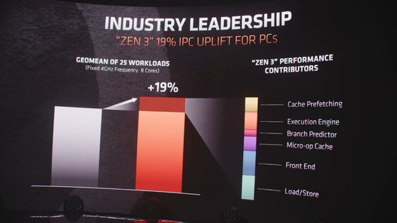
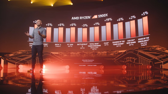
Compared to the Zen 2 CPU, which was just released in mid-2019, the Zen 3 CPU has a 19% increase in instruction per cycle (IPC). This is a phenomenal achievement, focusing on what I call 'hardcore engineering' and the team will continue to do so.
Q: Q:
To emphasize this '19% value', not only is the performance per clock improved by 19% compared to Zen 2, but also a new core complex that includes '8 cores' and '32MB L3 cache' ( CCX) was highlighted in AMD's announcement. CCX is AMD's unique unit that configures '4 cores, 8 threads + 8MB L3 cache' as one CPU module in Zen microarchitecture. In ' Ryzen 3 3300X ' announced in April 2020, CCX has been changed to '4 cores, 8 threads + 16MB L3 cache', and in Zen 3 architecture, it has been changed to '8 cores, 16 threads + 32MB L3 cache'.
How much has this new CCX design helped improve the original performance? Also, are there any other major benefits to CPU design by migrating to the newly integrated CCX?
Papermaster CTO:
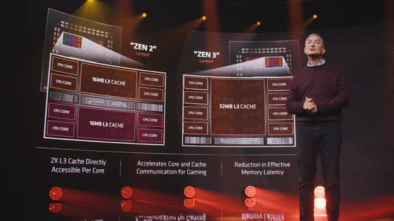
The CCX basic configuration changes were very important in gaming to reduce the huge amount of memory delay. Gaming applications are very important in the high performance desktop PC market. And its performance is highly dependent on the available L3 cache. This is because even if it hits the local L3 cache, it obviously doesn't follow the main memory reference.
As a result, we were able to reorganize CCX and double the four cores that have direct access to the 16MB L3 cache to eight cores that have direct access to the 32MB L3 cache. This is the best way to reduce latency. Obviously hitting the cache will give you an effective delay. This directly improves performance.
Q: Q:
Doubling the L3 cache access for each core from 16MB to 32MB is a huge leap forward. The overall delay has been improved up to 32MB, eliminating the need to access main memory. But does doubling the size affect the delay range of L3? Doubling the L3 cache makes a clear trade-off, even if you have more cores accessing it.
Papermaster CTO:
The development team did a great job in engineering, both logically and physically. The key is 'how to design the reorganization' and 'change the logic that supports the new structure and focus on the physical implementation as well'. The Zen 3 core reorganization had great engineering that really brought the benefits of reduced latency.
Generally, increasing the number of cores increases power consumption. Also, the technology node remained unchanged and remained in the 7nm process. The development team did the extraordinary task of managing every aspect of the implementation, not just managing the new CCX, keeping Zen 3 with a power envelope similar to Zen 2. As a result, it delivers enormous performance improvements while maintaining the same AM4 socket and the same power envelope.
Q: Q:
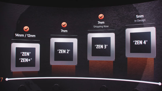
Speaking of process nodes, TSMC's 7nm was used in the Zen 3 architecture. For example, the Ryzen 3000XT is said to have adopted a minor update of the manufacturing process. Are there any additional benefits that the Ryzen 5000 can get through the manufacturing process?
Papermaster CTO:
In reality, the cores are on the same 7nm node, which means they have the same Process Design Kit (PDK). Looking at the transistors, the design guidelines from the manufacturing plant are the same. Of course, any semiconductor manufacturing node can adjust the manufacturing process to improve yields and more. Every quarter, process variability decreases over time. That's what is called a 'minor variation' of 7nm.

Q: Q:
Moving from Zen 2 to Zen 3 shows a 24% improvement in performance per watt. This clearly means that additional enhancements have been made at the power supply level.
Papermaster CTO:
We have put a great deal of effort into power management. We have a CPU-wide microcontroller and power management scheme. That's why we're very proud of what the Zen 3 development team has done to achieve a 24% power improvement. It's a further evolution of Precision Boost as a whole to give you more control over both frequency and voltage while always listening to the myriad of sensors on the chip. This enables power management tailored to the user's workload running on the microprocessor. In other words, it is highly responsive and efficient.
Q: Q:
One of the points pointed out in Zen 2 was the relatively high standby power consumption of the I / O dies, which ranged from 13 to 20 watts. The Zen 3 architecture is said to use the same I / O dies as Zen 2. Regarding AMD's goals for I / O and power consumption, AMD supports PCI Express 4.0 at 7nm , while I / O dies are based on GlobalFoundries ' 12 / 14nm process. Do you think I / O will be the key to Ryzen's future improvements?
Papermaster CTO:
This is a generational thing, and if we look to the future, we are driving improvements for all generations. As a result, AMD will move to PCI Express 5.0 and the entire ecosystem. Expect us to report on improvements to both next-generation I / O and memory controllers , as well as next-generation cores under design, at the next stage.
Q: Q:
While the both client and enterprise x86 architecture CPU markets are highly competitive, it is undeniable that there is increasing pressure from the Arm ecosystem in both markets. Currently, Arm's unique Neoverse V1 design promises to deliver near-x86 levels of IPC and a 30% year-over-year performance improvement with just a fraction of the power that x86 runs. So far AMD's goal has been to achieve peak performance like Zen 3, but how will AMD, which promises higher performance, especially on the roadmap, compete with Arm? is it?
Papermaster CTO:
We try not to step on the accelerator in terms of performance. It is not an instruction set architecture (ISA) issue. With any ISA, once you aim for high performance, you will need to add transistors to achieve that performance. There are some differences between ISA and other ISAs, but that's not the basics. We chose x86 for our design because of the huge software installation base and the huge toolchain there. This paved the way for the earliest adoption in the industry. We have historically lived in a competitive environment, but I don't think it will change in the future. Our view is that 'the greatest defense is an attack.'
Q: Q:
With the huge improvement in raw performance with Zen 3, there isn't much talk about how AMD is approaching CPU-based AI acceleration. Does it simply mean that it has this many cores and has strong floating-point arithmetic performance, or does it have acceleration and an optimized instruction range?
Papermaster CTO:
In Zen 3, the emphasis was on raw performance. Zen 2 had leadership performance in many areas, but the move to Zen 3 was aimed at achieving absolute leadership in performance.
Therefore, improvements in floating-point and multiply-accumulate operations will be able to support AI workloads such as vector workloads and inference. This makes it possible to handle a wide range of workloads. Also, the maximum boost frequency has been increased so that 'the rising tide lifts all ships '. However, we have not announced a new math format at this time.
Q: Q:
So does AMD already have an acceleration library for Zen 3 for AI workloads?
Papermaster CTO:
Yes, it is. We have a math kernel library that optimizes around Zen 3. This will be rolled out year by year.
Q: Q:
AMD is also expanding into other markets that previously did not have a high market share, such as Chromebooks and AMD's original Zen architecture embedded technology. Will AMD continue to focus on these markets? Or is there a possibility of untapped markets that AMD hasn't specifically addressed, such as IoT and automotive?
Papermaster CTO:
We continue to focus on closer markets compared to current markets. We have been expanding our market share in embedded devices, and AMD is focusing on this. What we're not doing is pursuing a market that may not have the media attention, but is incredibly unmatched by the high performance that AMD has. We want to provide the industry with valuable high performance, and we will focus on gaining market share in what we can offer as truly valuable.
Related Posts:
in Hardware, Posted by log1i_yk