``Inside the miracle of modern chip manufacturing'' that shows at a glance how much semiconductor technology has evolved
by
Semiconductor components installed in a variety of things, from smartphones to cars, are indispensable to modern life, and semiconductor manufacturing technology is constantly evolving to improve performance. The Financial Times publishes a column called ``Inside the miracle of modern chip manufacturing'' that visualizes and summarizes how semiconductor technology is evolving in an easy-to-understand manner.
Inside the miracle of modern chip manufacturing
https://ig.ft.com/microchips/
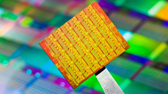
Semiconductor components installed in smartphones, PCs, and home appliances are basically made up of 'transistors' that control the flow of electricity. The smallest transistor has a size of about 50 nm, which is smaller than bacteria (about 1 μm) and viruses (about 300 nm).

This transistor with a size of 50 nanometers has the following configuration. An insulating material is layered on a silicon substrate, and a circuit is mounted using gates, metal contacts, and metal interconnects.
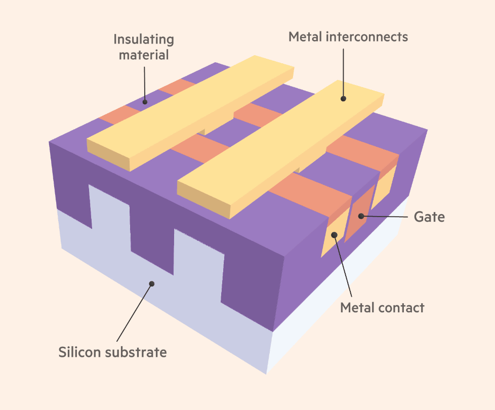
The three-dimensional structure and shape of this transistor allows for the construction of high-density integrated circuits.

The Financial Times says, ``Intel, Samsung, and TSMC are the only three companies in the world that can mass-produce 50-nanometer-class transistors.'' For example, the A17 Pro chip installed in the iPhone 15 Pro is said to be manufactured using the '3nm process.' This process used to refer to the minimum wiring pitch (spacing), but now, due to the convenience of transistor design, it no longer indicates physical dimensions, but simply the technology generation. Ta.
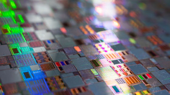
It is possible to arrange 200 million transistors in just 1 square mm, and the number of transistors in an entire integrated circuit is in the tens of billions. Manufacturers are aiming to increase transistor density in the future so that a single chip can contain more than 1 trillion transistors.
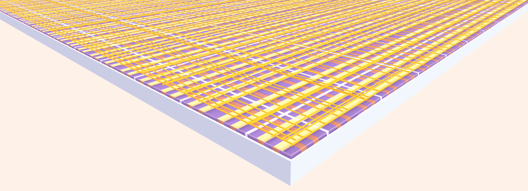
Countless transistors are interconnected on a single integrated circuit. It is said that the length of a single wire can reach approximately 500km.

To increase the number of transistors on a chip, companies are competing to improve both manufacturing and design techniques. Semiconductor fabs TSMC and Samsung continue to research manufacturing technology, and NVIDIA and AMD continue to research design technology. In addition, Intel has declared that it will focus not only on chip design but also on semiconductor manufacturing business, and has announced plans to realize a 10A process node equivalent to 1nm in 2027.
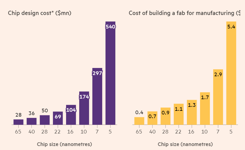
Of course, as manufacturing and design technology advances, the cost of designing and manufacturing chips is becoming more and more expensive. The bar graph below shows the chip design cost (purple) and manufacturing cost (yellow) for each generation. In both cases, you can see that the cost increases as the generation of process rules progresses.
Gordon Moore, co-founder of Intel, proposed ``
Intel's CEO says Moore's law has slowed down from the traditional 2 to 3 year pace but is not dead yet - GIGAZINE

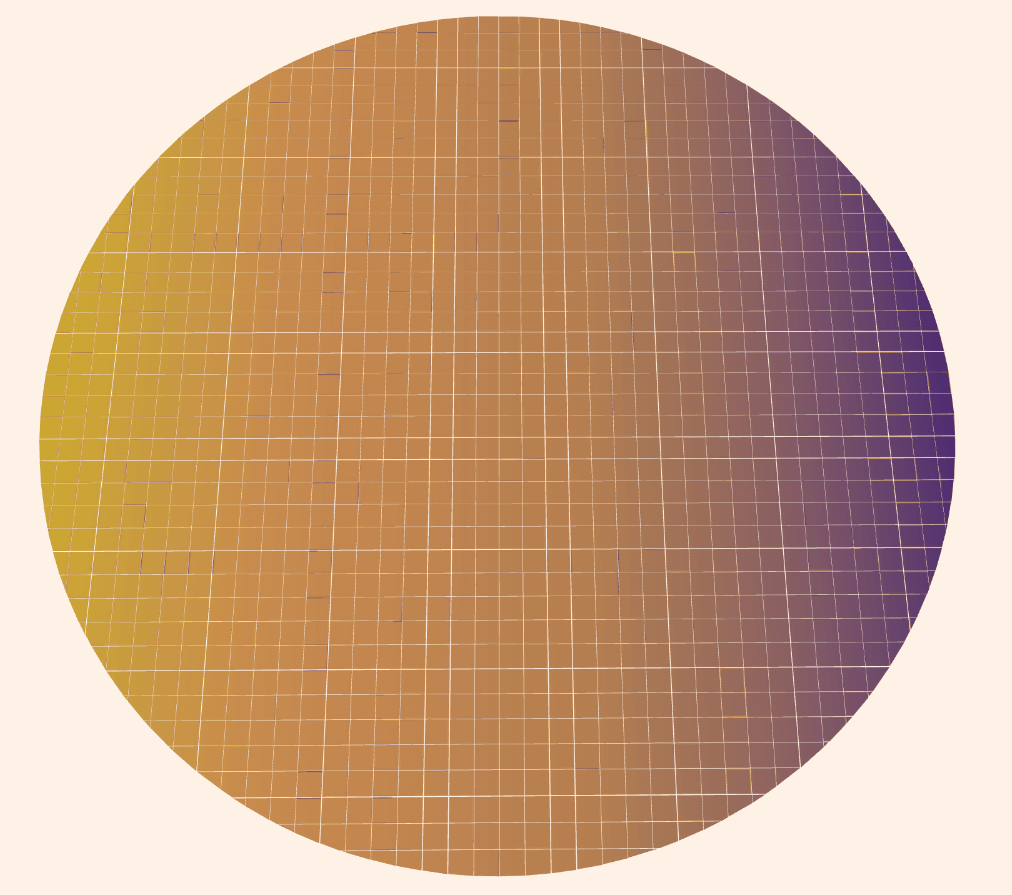
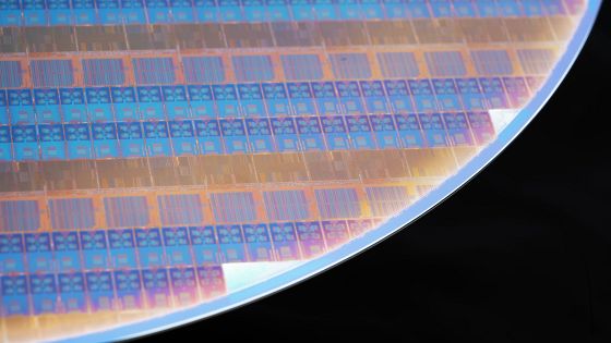
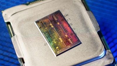
These integrated circuits are made from wafers made by thinly slicing blocks of silicon.
You can understand how chips are made from silicon by reading the following article.
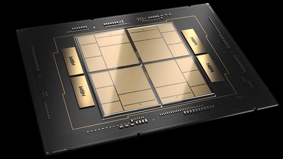
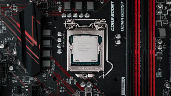
Packaging then shapes the manufactured chips into a form suitable for electronic devices. In recent years, it has become mainstream to assemble transistors by arranging them three-dimensionally, rather than arranging them on a flat surface. There has also been a shift from ``system-on-chip (SoC),'' in which the entire processor is built on a single silicon, to ``multi-chip module (MCM),'' in which multiple chips are mounted on a single die. I am.
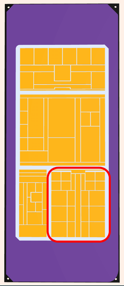
For example, Intel's Meteor Lake generation of microprocessors is constructed by placing tiles of chiplets on a silicon substrate. The overall size of the package is 50mm x 25mm.
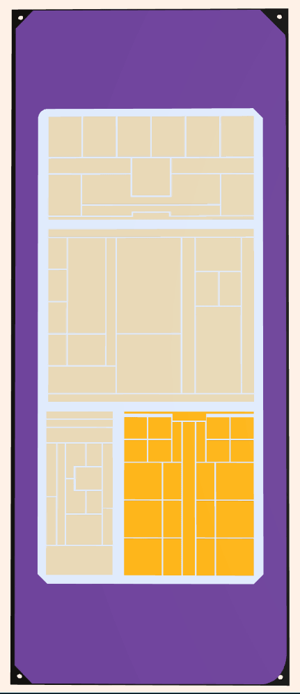
At the top is a 'graphic tile' that handles graphics-related processing.
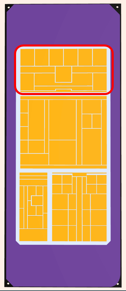
Below that is the 'system tile' that is responsible for memory control and AI processing.
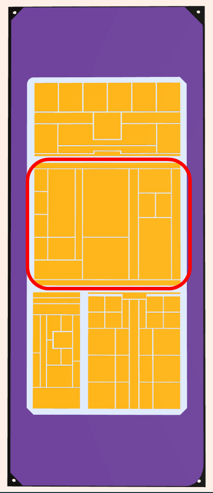
The 'I/O tile' is responsible for connectivity, allowing components to communicate efficiently with each other and with connected external entities.
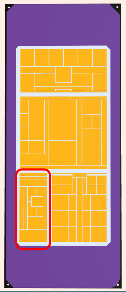
The 'computing tile' is the so-called CPU and monitors performance and efficiency.
This MCM package structure is said to be a way to keep Moore's law alive, and each company is designing in a similar direction. MCM is also highly flexible, allowing chiplets to be replaced according to requirements, allowing it to accommodate a variety of customers.
Furthermore, the structure of the transistor itself has been reviewed in recent years. In traditional chip architecture, signal wires and power wires are located on the surface of the silicon substrate. As a result, power lines and signal lines compete for space, causing heat generation and signal delays, leading to performance deterioration.
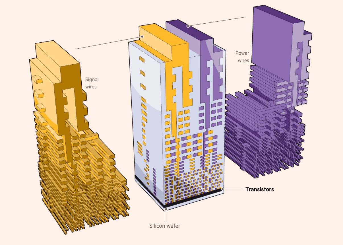
Therefore, semiconductor manufacturers are developing ``backside power supply technology'' that moves the power lines to the backside of the silicon substrate.
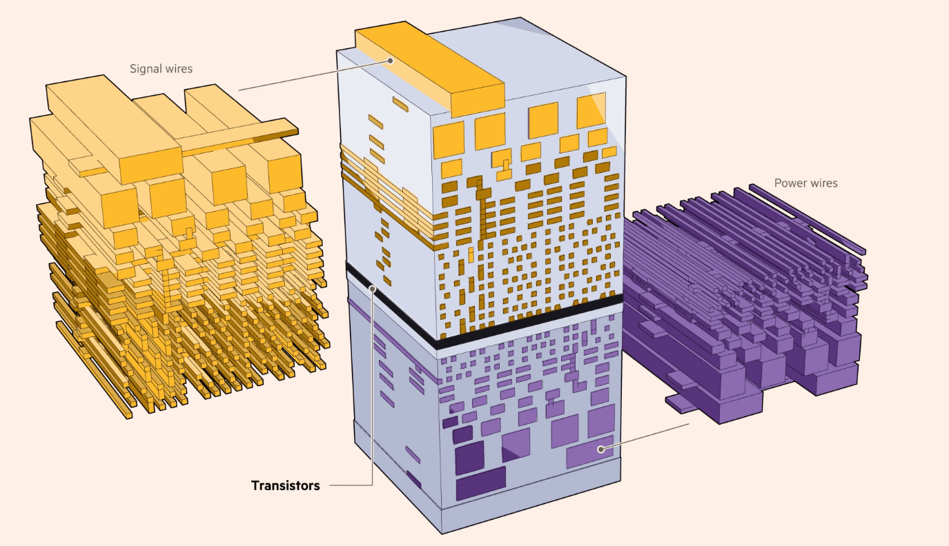
For example, Intel announced ``Intel PowerVia'' in 2023, which is a type of backside power supply technology, and Intel claimed that ``this technology will allow us to pack 1 trillion transistors into a package by 2030.''
Intel successfully tests ``PowerVia'', a backside power supply technology that restarts ``Moore's Law'', and Intel claims to be ``two years ahead of its rivals'' and ``stop making pizza'' - GIGAZINE
Furthermore, although current integrated circuits use electrons, semiconductor manufacturers are competing with each other to develop `` silicon photonics, '' which uses light-emitting elements and light receivers to create faster and more power-saving integrated circuits. Masu.
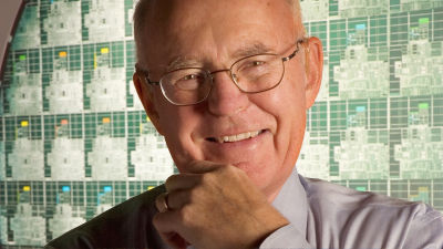
Chris Orth, Director of Intel's Advanced Transistor Development Division, said, ``Semiconductors are essential to our daily lives, and we take them for granted.'' I'm looking forward to seeing what we can do over the next 20 years.'
'TSMC's engineers are able to develop new generations of chips at a regular pace because customers want them,' said Ming Kao, vice president of pathfinding at TSMC. But that won't happen,' he said.
Related Posts:
in Hardware, Posted by log1i_yk