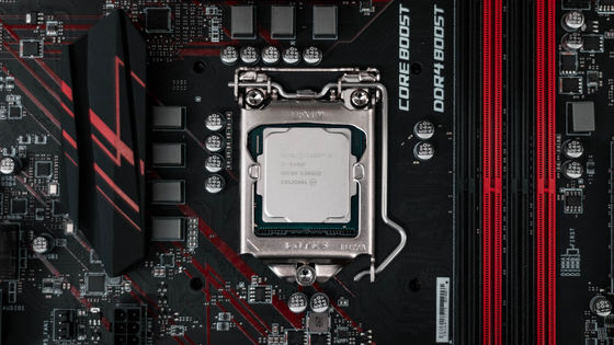
Three chip manufacturers, Intel, Samsung, and TSMC, announce demonstrations of the future three-dimensional transistor structure 'CFET'
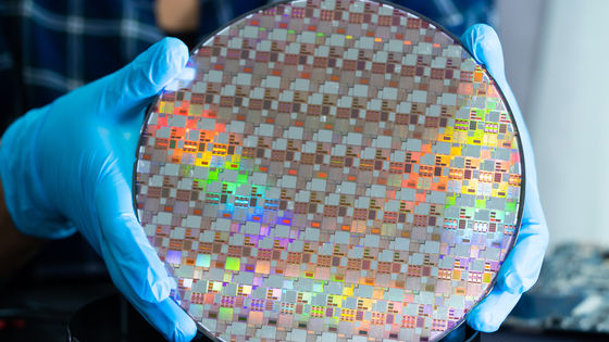
At the IEEE (Institute of Electrical and Electronics Engineers) International Electronic Devices Conference (IEDM) held in San Francisco from December 9th to 13th, 2023, Intel, Samsung, and TSMC announced the use of CFET (complementary technology), a technology for miniaturizing CMOS memory. We have released demos of ``type field effect transistors'' .
Intel, Samsung, and TSMC Demo 3D-Stacked Transistors - IEEE Spectrum
Intel Demos 3D Transistors, RibbonFET, and PowerVia Technologies | TechPowerUp
https://www.techpowerup.com/316589/intel-demos-3d-transistors-ribbonfet-and-powervia-technologies
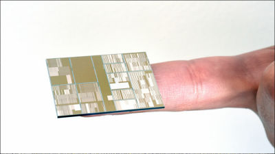
Intel was the first to demonstrate CFET, announcing an early version at IEDM in 2020. This time, Intel has reported several improvements to the CMOS inverter, which is the simplest circuit in the CFET, and Marko Radosavljevic, chief engineer of Intel's Component Research Group, said, ``The inverter is simple. It is done in layers and can reduce the size by up to 50% from regular CMOS inverters.'
Intel announced in June 2023 that it will implement a technology called ' Intel PowerVia ' into production test chips. This Intel PowerVia allows power to be supplied from the back side of the transistor layer, greatly simplifying the circuit. As a result, it seems that the CMOS inverter was able to reduce the gate pitch of the transistor called CPP (contact poly pitch) to 60 nm. Intel says this PowerVia technology is already ready for mass production and plans to release products equipped with it in 2024.
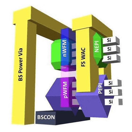
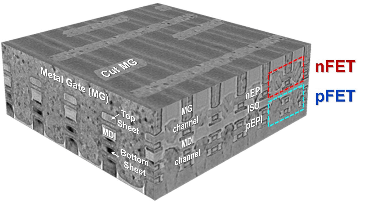
In addition, Intel is increasing the number of nanosheet transistors per device from two to three layers, reducing the pitch between devices from 50nm to 30nm, and using improved geometries in the device connections to improve the CFET's electrical It is reported that the characteristics have been improved.
In addition, when Intel reviewed its process rules in 2021, it stated that after FinFET, it would introduce ``RibbonFET'' that adopts a gate all-around nanosheet structure in the future.
Intel technology executives talk about Intel's revised process rules and new roadmap - GIGAZINE
At this IEDM, Intel also demonstrated RibbonFETs, reporting faster switching speeds for transistors, leading to increased frequency and performance.

Samsung has announced that it has been able to shrink CPP to 48nm or 45nm. Among Samsung's prototype CFETs, the one with a CPP of 45 nm showed a decrease in performance, but Samsung says the problem can be resolved by optimizing the manufacturing process. By improving chemical etching, Samsung achieved isolation between nFET and pFET, and at the same time was able to improve device yield rate by 80%.
Furthermore, like Intel, Samsung has adopted technology that allows power to be supplied from the back side of the transistor layer. However, while Intel uses three layers of nanosheets, Samsung uses one layer of nanosheet transistors. Samsung claimed that increasing the number of nanosheet transistors would further improve the performance of the CFET.
TSMC also reported that by devising the etching of nanosheet transistors, they were able to efficiently build an insulating layer on nanosheets and successfully reach a level of CPP of 48nm.
Although each manufacturer is developing technology to put CFET into practical use, it is expected that CFET will not be commercially deployed until 2030 at the earliest.
Related Posts:


in Hardware, Posted by log1i_yk