IBM and Samsung announce a new semiconductor design that will lead to the realization of a 'smartphone with a battery that lasts for a week', a new idea of 'stacking transistors vertically'
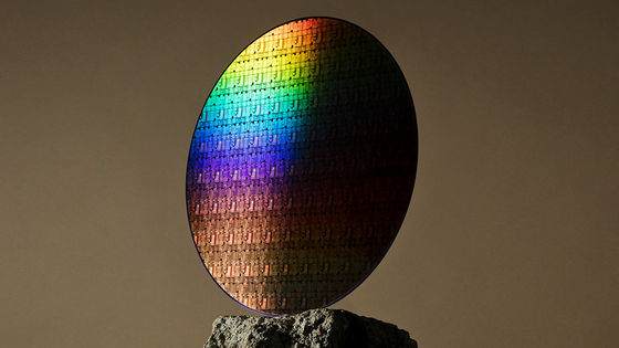
On December 14, 2021 local time, IBM announced a new semiconductor design ' Vertical Transport Field Effect Transistors (VTFET) ' with the idea of 'stacking transistors vertically' jointly developed with Samsung. VTFET has the potential to double the performance per power consumption and reduce energy consumption by 85% compared to the conventional design, and it is said that it will lead to the realization of 'a smartphone that has a battery for one week without charging'. increase.
IBM and Samsung Unveil Semiconductor Breakthrough That Defies Conventional Design
IBM and Samsung say their new chip design could lead to week-long battery life on phones --The Verge
https://www.theverge.com/2021/12/14/22834895/ibm-samsung-vtfet-transistor-technology-advancement-battery-life-smartphone-semiconductor
IBM and Samsung detail'breakthrough' vertical transistor architecture --SiliconANGLE
https://siliconangle.com/2021/12/15/ibm-samsung-detail-breakthrough-vertical-transistor-architecture/
IBM and Samsung Unveil Vertical Transistor Architecture
https://www.hpcwire.com/off-the-wire/ibm-and-samsung-unveil-semiconductor-breakthrough/
IBM and Samsung have newly jointly developed a semiconductor design with a style of 'stacking transistors vertically', which is fundamentally different from the existing method of 'arranging transistors on a plane'. The official movie that explains what kind of design it is is below.
IBM and Samsung Unveil Semiconductor Breakthrough That Defies Conventional Design --YouTube
A transistor is a type of semiconductor element . Simply put, the greater the number of transistors on a wafer , the higher the performance of the chip.

The newly developed VTFET is designed to allow current to flow perpendicular to the wafer by stacking transistors in layers on the wafer. According to the announcement, this design can alleviate physical restrictions such as transistor gate length, spacer thickness, and contact size. Semiconductor design with the design concept of 'stacking vertically' is not new, but until now, the method of stacking chip components vertically instead of transistors has been the mainstream.
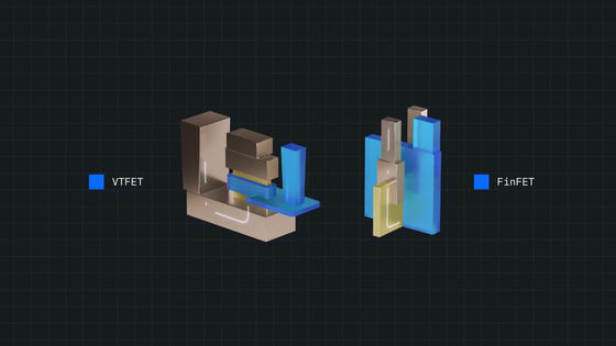
By relaxing this physical constraint, it is possible that the performance per power consumption will be doubled and the energy consumption will be reduced by 85% compared to the existing FinFET design.
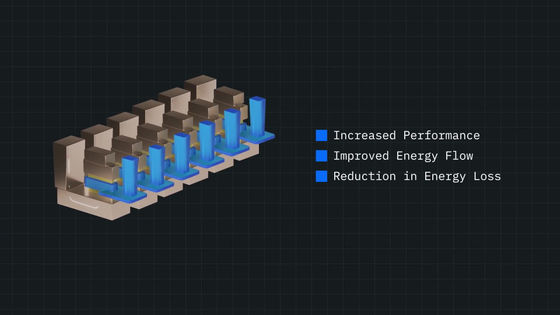
VTFETs can reduce carbon dioxide emissions through smartphones and energy-intensive processes that batteries have for a week without charging, and by reducing energy consumption, marine buoys, self-driving cars, space shuttles, etc. IBM claims that it will be possible to install

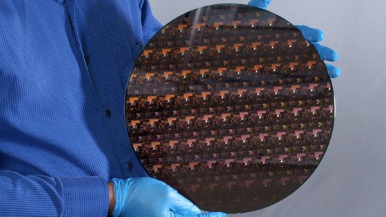
IBM succeeded in manufacturing the world's first 2nm process chip in May 2021, and commented that it 'opened a new way to continue Moore's Law' together with this VTFET. I am.
IBM manufactures the world's first '2nm process chip', 45% performance improvement & 75% reduction in power consumption compared to 7nm-GIGAZINE
Related Posts:
