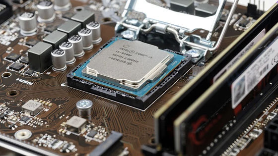
Intel begins initial production of 18A (1.8nm) process semiconductors
Intel plans to start mass production of semiconductors using the 18A (1.8nm) process in 2025. Intel Engineering Manager Pankaj Maria recently reported that the company has successfully completed initial production of the 18A process.
Initial Intel 18A Node Wafer Run Lands in Arizona Site, High-Volume Manufacturing Could Start Earlier Than Expected | TechPowerUp
Intel reaches 'exciting milestone' for 18A 1.8nm-class wafers with first run at Arizona fab | Tom's Hardware
https://www.tomshardware.com/tech-industry/intel-reaches-exciting-milestone-for-18a-1-8nm-class-wafers-with-first-run-at-arizona-fab
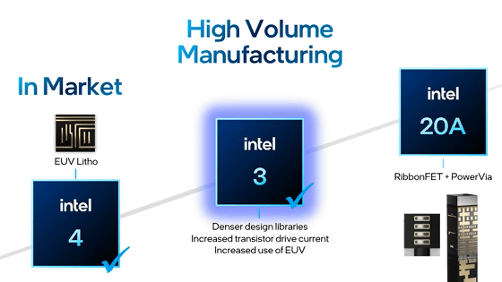
Intel has been accelerating research and development of semiconductor miniaturization technology by announcing the slogan '5 process nodes in 4 years (5N4Y)' in 2021. Looking at the roadmap shown by Intel, we can see that it planned to complete the development of 18A by 2024.

In August 2024, Intel announced that development of the 18A was progressing smoothly and declared that production of the consumer processor 'Panther Lake' and server processor 'Clearwater Forest' using the 18A would begin in 2025.
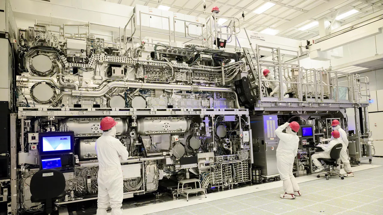
Then, on March 17, 2025, Engineering Manager Pankaj Maria revealed in a post on his LinkedIn account that initial production of the 18A had begun. At the time of writing, Maria's post was hidden, but overseas media TechPowerUp has published a screenshot of the post.

According to Maria's post, the 18A process semiconductors are produced in a factory in Arizona. Maria said, 'The eagle (the national bird of the United States) has landed,' highlighting the fact that the world's smallest class semiconductors are being produced in the United States.
Related Posts:


in Hardware, Posted by log1o_hf