Huawei is building a vast chip equipment R&D center in Shanghai, China, hiring many engineers who already worked at ASML, TSMC, etc.
by
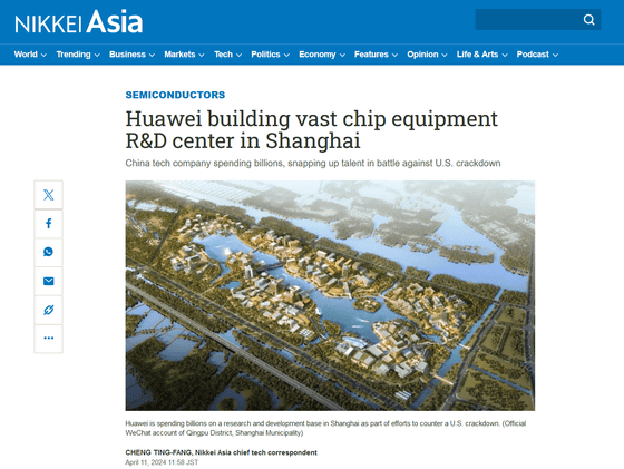
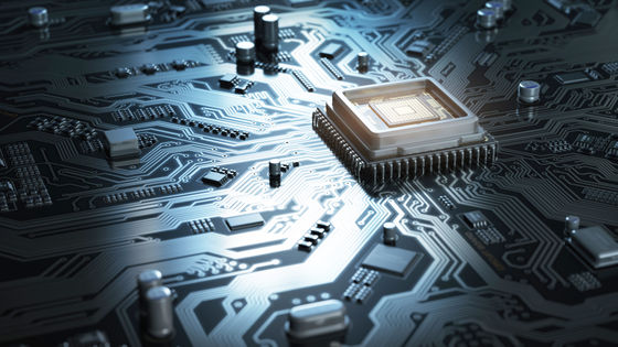
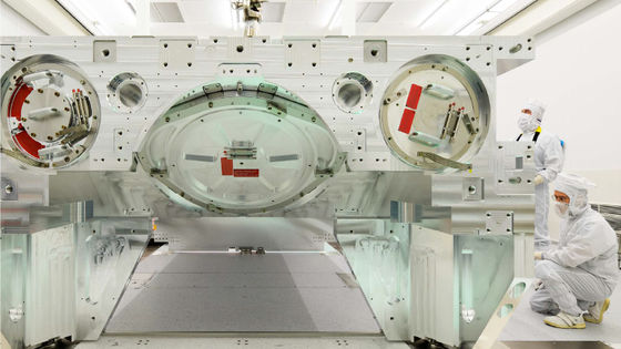
Huawei is building a large-scale semiconductor equipment research and development center in the Qingpu district of Shanghai, China, which will develop the lithography equipment needed to manufacture cutting-edge chips, Nikkei Asia reports.
Huawei building vast chip equipment R&D center in Shanghai - Nikkei Asia
https://asia.nikkei.com/Business/Tech/Semiconductors/Huawei-building-vast-chip-equipment-RD-center-in-Shanghai
Huawei wants to develop lithography machinery at new Shanghai chip R&D campus - DCD
https://www.datacenterdynamics.com/en/news/huawei-wants-to-develop-lithography-machinery-at-new-shanghai-chip-rd-campus/
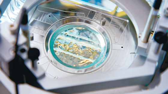
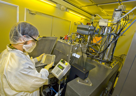
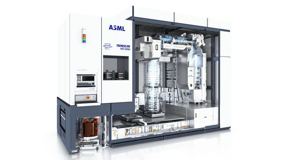
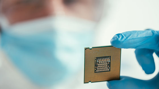
Huawei will be working on developing lithography equipment at the research and development center currently under construction. Lithography equipment is a device that prints circuit patterns onto silicon wafers and is essential for producing cutting-edge chips. The production of lithography equipment is monopolized by ASML of the Netherlands, Nikon and Canon of Japan, and ASML of the Netherlands has a near monopoly on the production of EUV lithography equipment, which is necessary for next-generation semiconductors.
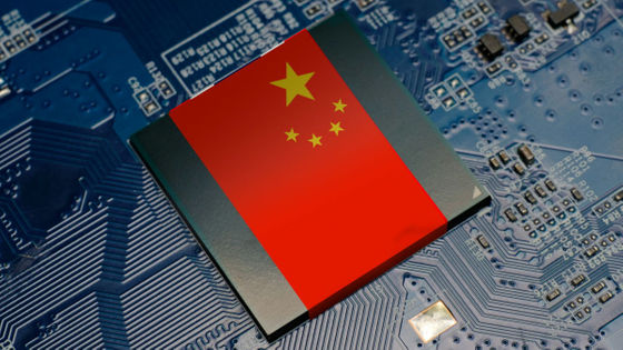
However, because the United States is pressuring manufacturers such as ASML not to sell lithography equipment to China, it is very difficult for Chinese company Huawei to procure cutting-edge lithography equipment through legitimate means. Therefore, Huawei is trying to develop its own lithography equipment.
US requests semiconductor lithography equipment manufacturer ASML to stop sales to China - GIGAZINE
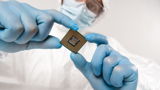
Developing lithography equipment requires a huge budget and experienced personnel. Huawei's research and development expenditures in 2023 will be a record high of 164.7 billion yuan (about 2.5 trillion yen), which is equivalent to 23.4% of Huawei's total revenue. The fact that Huawei is investing about a quarter of its total revenue in research and development shows that the company is particularly focused on technological innovation.
According to Nikkei Asia, Huawei is offering employees at the R&D center salaries that are about twice as much as local chipmakers, and is particularly looking for veteran engineers who have worked at TSMC, ASML, Intel, Micron, and other companies. Huawei is showing its willingness to invest in labor costs in order to hire experienced veteran engineers.
by Berkeley Lab
However, even with the abundance of talent, the working environment seems to be quite harsh. In China, the harsh working system known as '996' has become a social problem, but at Huawei, the even harsher '007' is the norm. '996' means '9am to 9pm, 6 days a week,' but Huawei's '007' means '00am to 00am, 7 days a week.' According to a former Huawei engineer, although the contract period with Huawei is three years, most people quit before the contract is renewed, suggesting that Huawei's research and development center may also have a very harsh working environment.
The R&D center that Huawei plans to build will house Huawei's chip development center and the headquarters of HiSilicon, a fabless subsidiary of Huawei. The Shanghai Municipal Government has announced that Huawei's total investment in the R&D center in Shanghai's Qingpu District will be about 12 billion yuan (about 254 billion yen).

◆ Forum is currently open
A forum related to this article has been set up on the official GIGAZINE Discord server . Anyone can post freely, so please feel free to comment! If you do not have a Discord account, please refer to the account creation procedure explanation article to create an account!
Discord | 'Do you think Huawei will be able to manufacture advanced chips that can compete with TSMC and Samsung?' | GIGAZINE
https://discord.com/channels/1037961069903216680/1228274518645014549
Related Posts:

in Hardware, Posted by log1i_yk