Why does the US Department of Defense DARPA invest a huge cost to make the latest chip with old process rules?
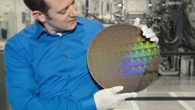
Samsung and TSMC are entering mass production of the latest chips which adopted the 7 nm process. Amidst the limits appearing in microfabrication technologies that have greatly contributed to the performance improvement of semiconductor chips until now, the DARPA research institute of the US Department of Defense intends to dare to use state-of-the-art equipment older than 15 years ago, It seems to be developing.
The Foundry at the Heart of DARPA's Plan to Let Old Fabs Beat New Ones - IEEE Spectrum
https://spectrum.ieee.org/nanoclast/semiconductors/processors/the-foundry-at-the-heart-of-darpas-plan-to-let-old-fabs-beat-new-ones
As the limits of Moore's Law are lost, semiconductor manufacturers still continue to push forward the development of miniaturization technology, enabling huge costs for technology development. Meanwhile, DARPA is pursuing semiconductor development by sticking to "old-fashioned" production facilities as if it goes against the trend of miniaturization.
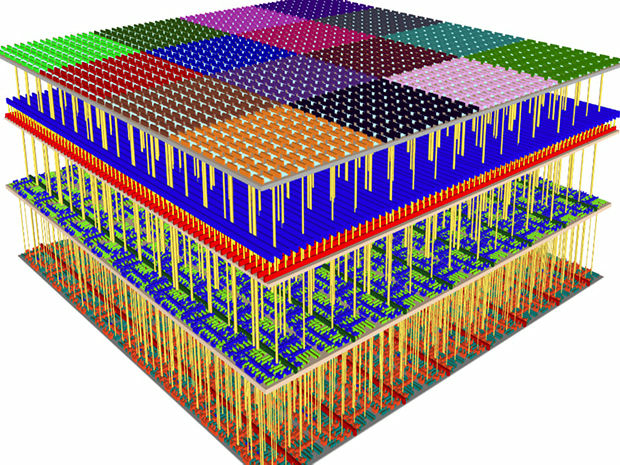
DARPA has allocated a budget of $ 41 million (about 4.6 billion yen) in the development project of "Computing system utilizing high-density, high-definition monolithic 3D integration technology". The semiconductor developed in this project is manufactured on a 200 mm silicon wafer using 90 nm process technology. This 90nm process was "state-of-the-art manufacturing technology" around 2004, but now it is "abandoned classical manufacturing technology".
DARPA has developed the aforementioned chip based on CMOS chip technology integrating 2 million carbon nanotubes developed by MIT and Stanford University and 1 million or more resistive RAM cells, and the technology adopted It itself is a state-of-the-art one. That's why we spend a great deal of money trying to commercialize it using state-of-the-art technology using old-fashioned manufacturing equipment that has been declining for 15 years.
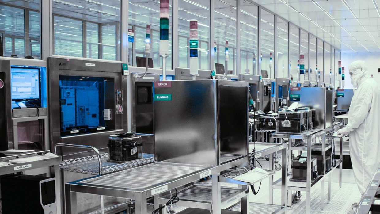
DARPA is one of the reasons for using old equipment is "reliability". According to Thomas Sonderman, CEO of SkyWater Technology Foundry who cooperates with DARPA, Thomas Sunderman said conventional technology is guaranteed high reliability and it is suitable for manufacturing relatively small chips. Therefore, it seems that many of government-related chips are manufactured at 90 nm process.
"Security reasons" can also be mentioned. The use of state-of-the-art technology may depend on specific expertise and is not suitable for the development of defense technology. Also, it is inappropriate to allow intervention by third part because it leads to risk of leakage of defense technology.
And one of the big reasons is "uniqueness" that it adopts unique technology that is not unique. Carbon nanotubes are used for semiconductor materials in the above-mentioned chips, but this is a material that is rarely used as a commercial semiconductor material. While it is desirable to complete the flow of manufacturing CMOS within one manufacturing facility, using unusual materials makes it difficult to share lines with other semiconductors due to "contamination" It is necessary to prepare your own equipment.

It is essential to develop state-of-the-art technologies such as extreme ultraviolet lithography with ultra-miniaturization technology of 7 nm or less, and development cost of miniaturization technology is rising year by year. If the research of DARPA which adopts the traditional manufacturing process succeeds, it seems that the manufacturing method is "returning to the 90 nm era" and it will also raise the semiconductor manufacturing technology.
Related Posts:


in Hardware, Posted by darkhorse_log