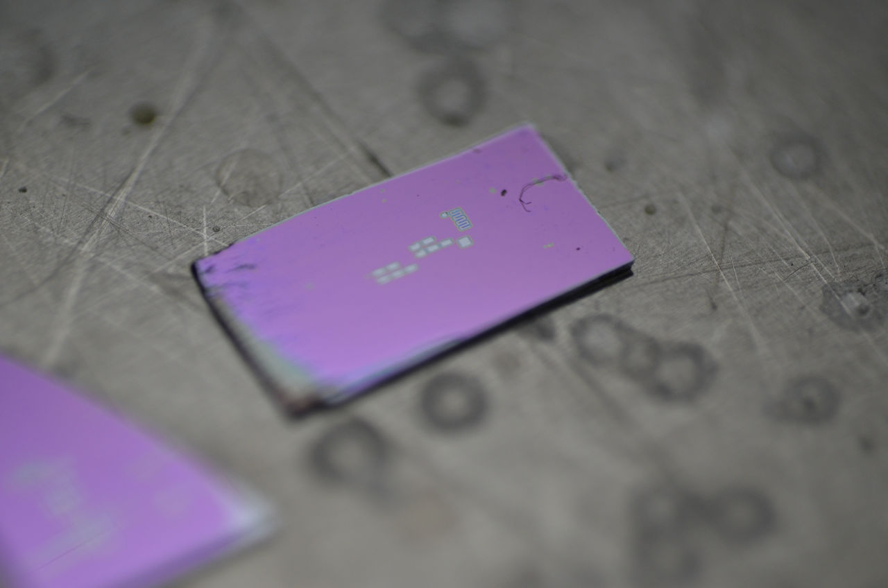
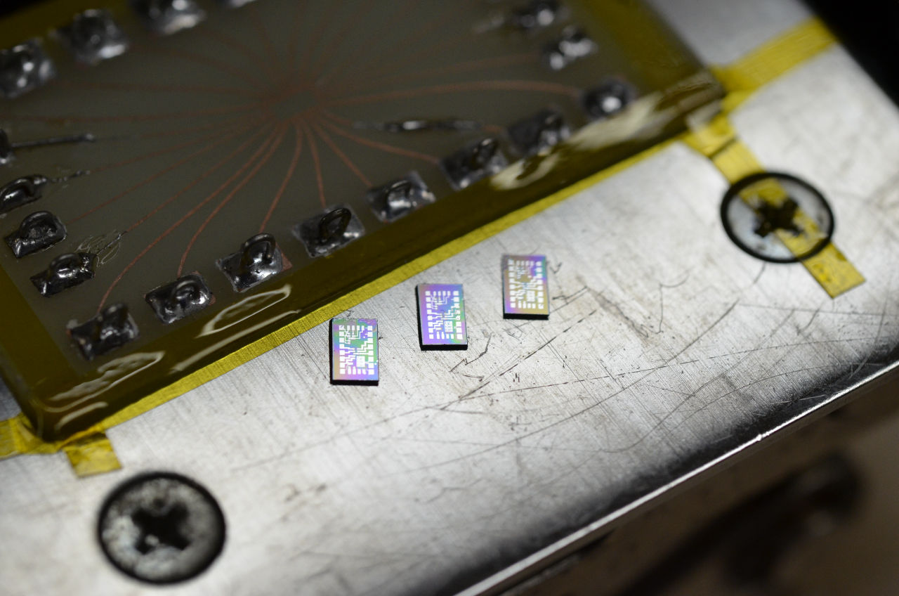
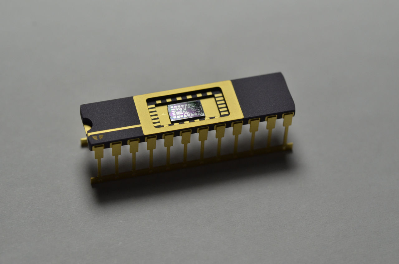
Tsuyomono which designs IC chips from scratch and even manufactures themselves appears, homemade chips look like this
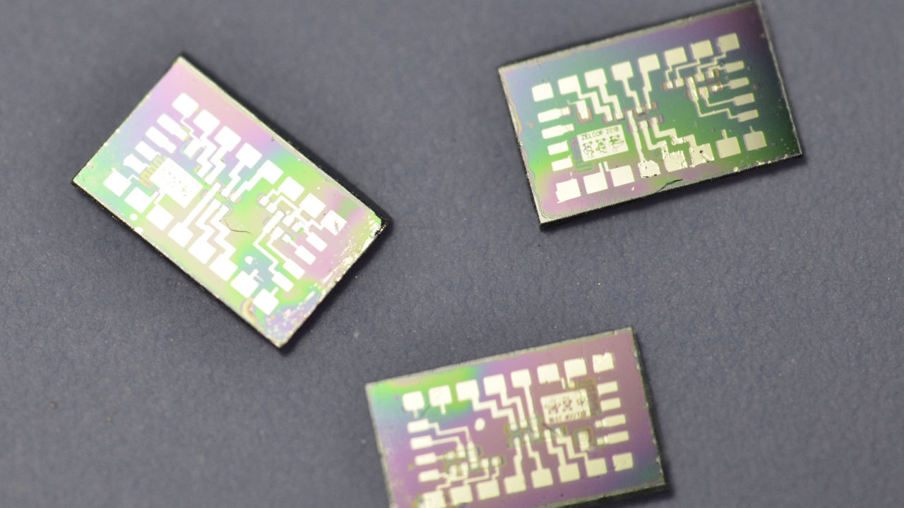
Integrated circuit(IC) is used for every kind of electronic equipment, it is mass-produced in a very sophisticated manufacturing factory. Tsumono that the IC chip was worked in the garage including the silicon mask, dope, vapor deposition, etching etc from the design appears, and it shows the state on the blog.
First IC :) - Sam Zeloof
http://sam.zeloof.xyz/first-ic/#
Sam Zeloff made IC chips at home garage. In the state of New Jersey, USA, he is offering services to support researchers such as universities to lend SEMs and create samples of sputtering. Mr. Zeroro made a challenge to design and manufacture IC chips from scratch using equipment in their own garage.
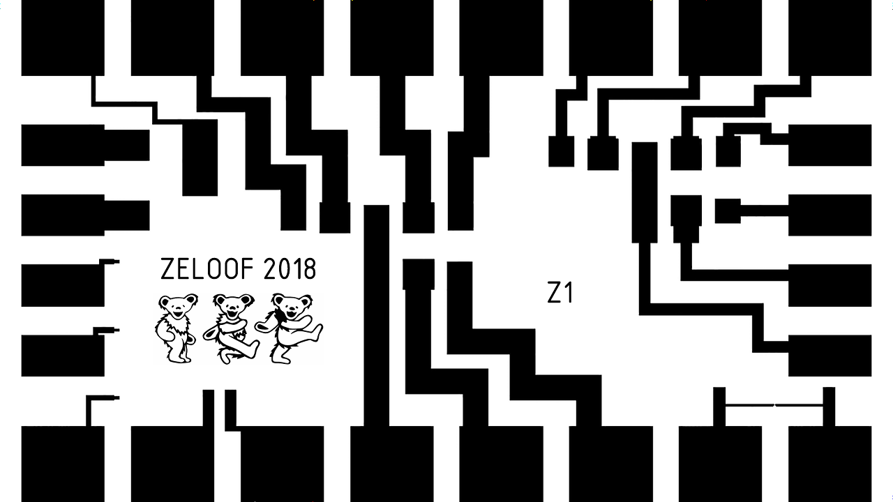
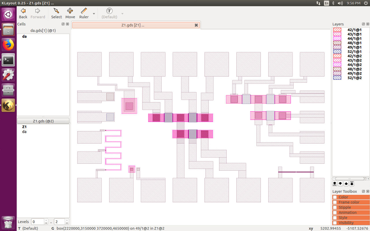
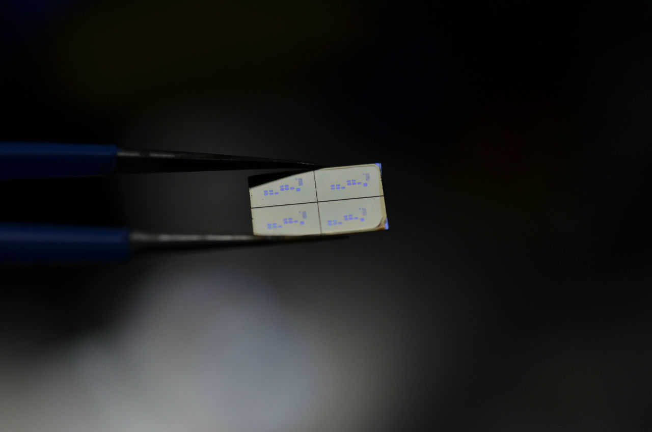
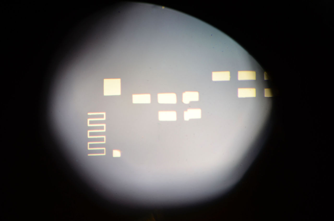
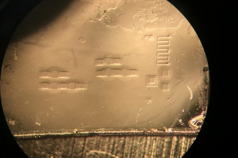
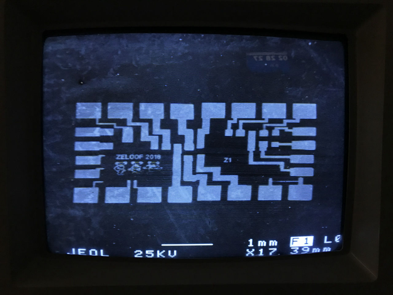
In the design of the IC chip "Z1"Magic VLSIWe used four masks of active / doped region, gate oxide film, contact window, top metal.

Active / doped region
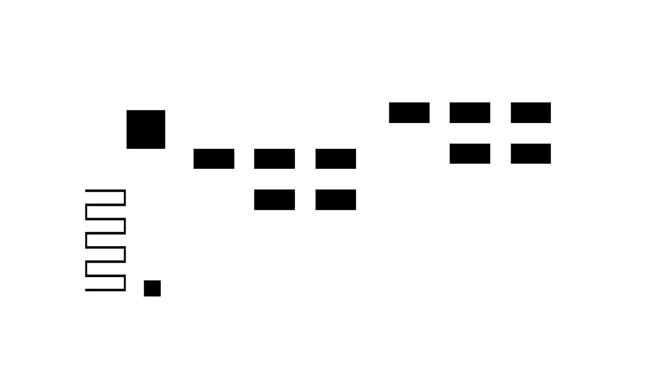
Gate oxide film

Contact window
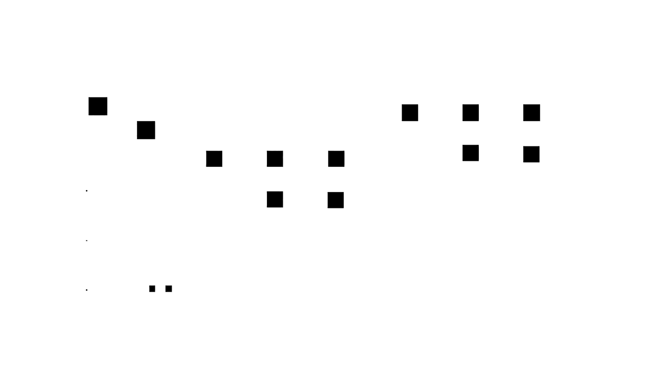
Top Metal
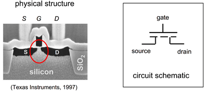
According to Xeloff, it is easy to make P-channel type MOS rather than N-channel type from the viewpoint of ion contamination by self-fabrication of IC chip in the garage. It seems that the mask was designed with an aspect ratio of 16: 9 all so that it can be projected easily.
It is said that the manufacturing process based on the design goes through 66 stages in IC chip manufacturing. It took about 12 hours in total to manufacture the IC chip, "The yield of the process depends to a large extent on the amount of coffee inthe day," Zeloff said, and seems to be quite persistent work.
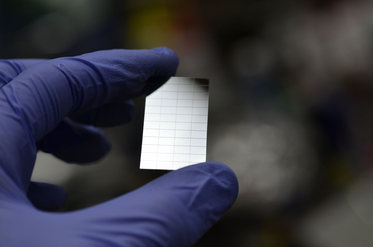
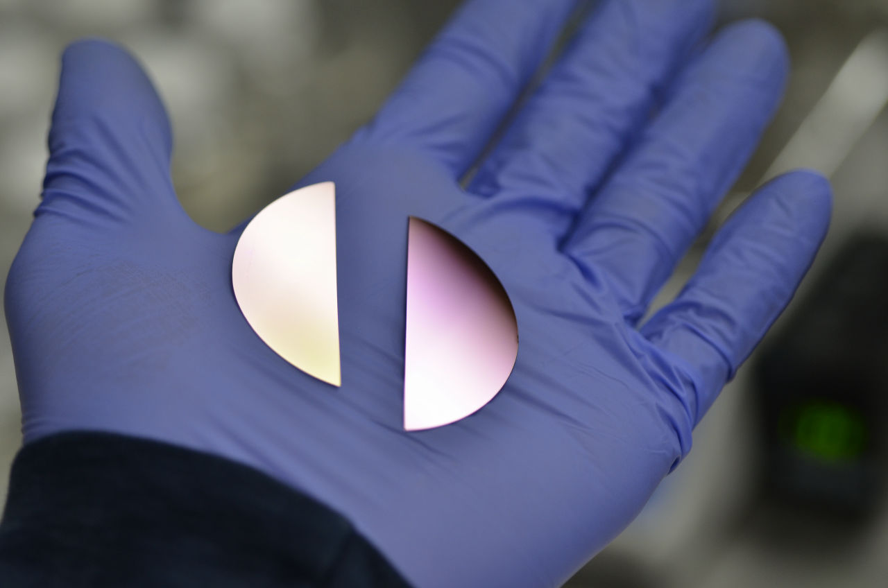
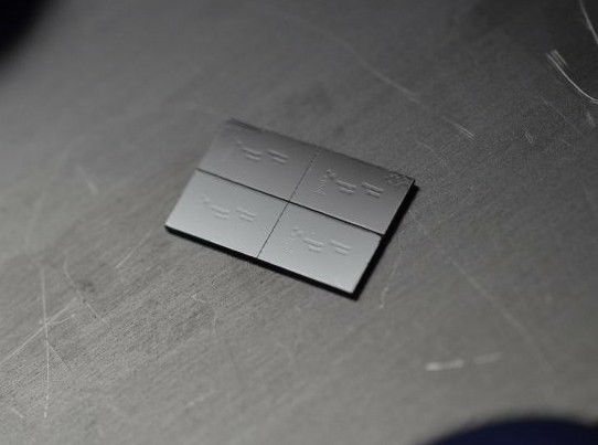
Using an Epilog fiber laser, cut a 50 mm N type silicon wafer into a 5.08 mm × 3.175 mm rectangle.
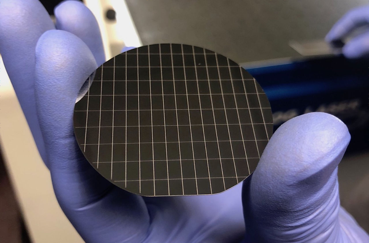
The die size is decided to be compatible with Kyocera 's 24 - pin DIP carrier.
After washing with piranha solution (H2SO4: H2O2), RCA1 (H2O: NH3: H2O2), RCA2 (H2O: HCL: H2O2), immerse it in a thin HF solution to make a natural oxide film.
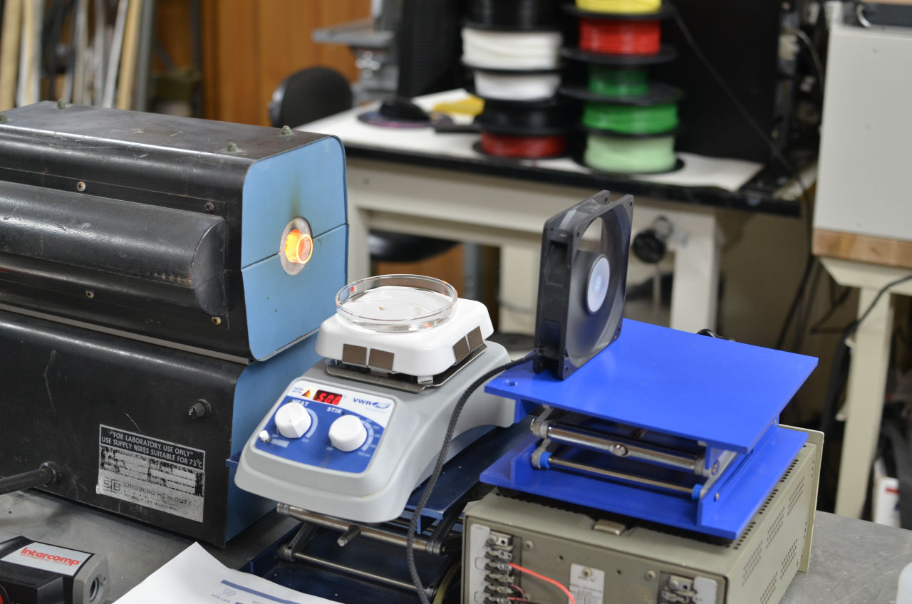
Field oxidation adopts wet oxidation by vapor deposition. The oxide film grows to a thickness of 5000 to 8000 Å (500 to 800 nm).
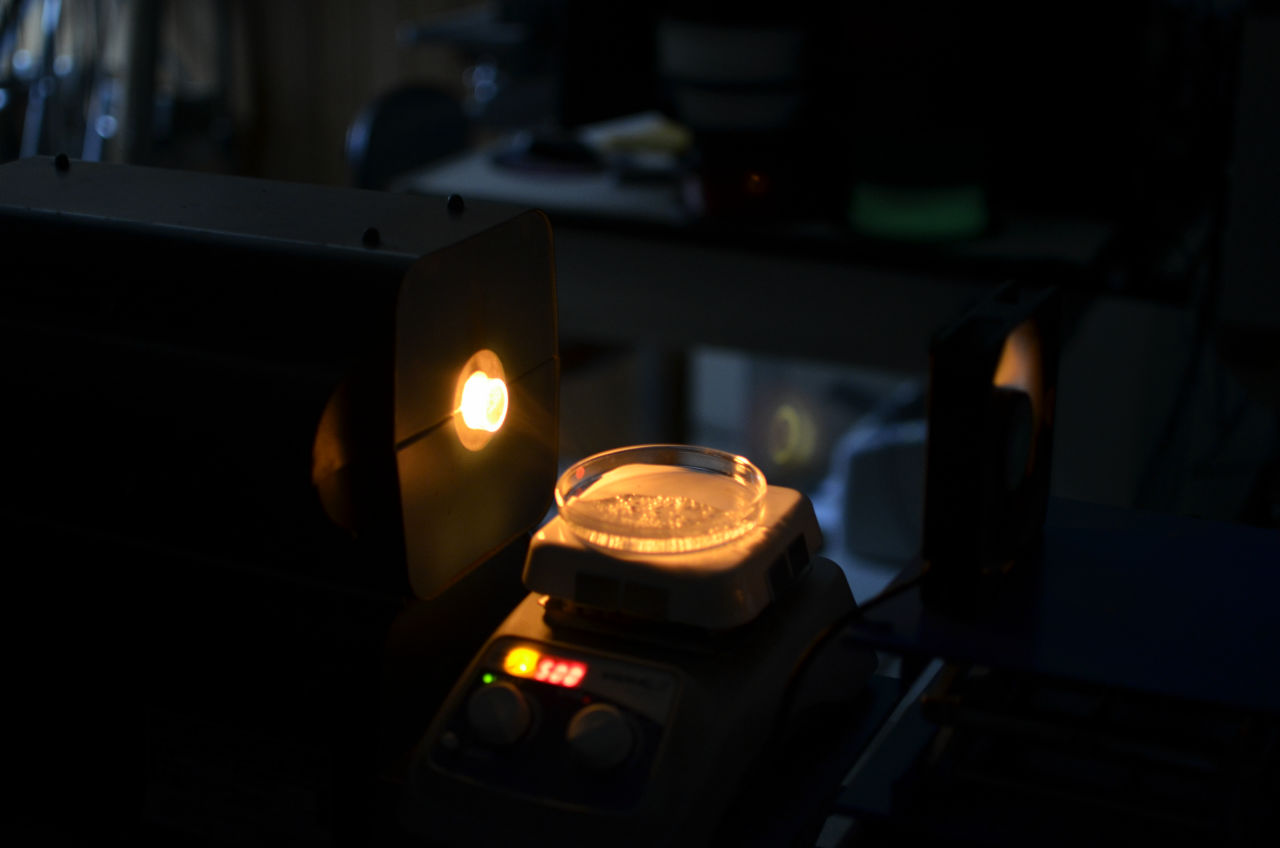
The oxidized wafer looks like this.
Resist pattern
Soft bake for 30 minutes on a 90 ° hot plate, then hard baked to transfer the oxide layer.
Then the process of lithography. Exposure the active area to Mark IV maskless photolithography stepper (365 nm) and soak in KOH solution.
Subsequently doping. The solid source is boron nitride, standard "Spin-On Glass & Spin-On Dopants Application ProcedureIt seems to be doped with.

Furthermore, repeat the patterning process twice for the gate oxide layer and twice for the contact layer. Since the entire wafer is oxidized in the doping process, it is necessary to drill a contact window in order to make contact with the source / drain doped region in the metal layer.
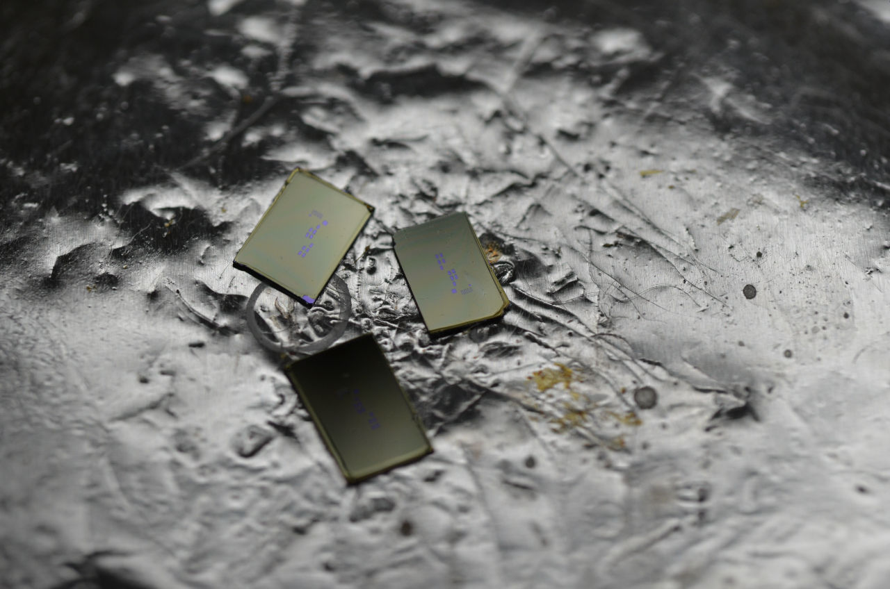
Once all the transistors are shaped and interconnected, the aluminum layerSputteringTo do.
The metal layer was patterned by photography and etched in high temperature phosphoric acid to complete the IC chip.

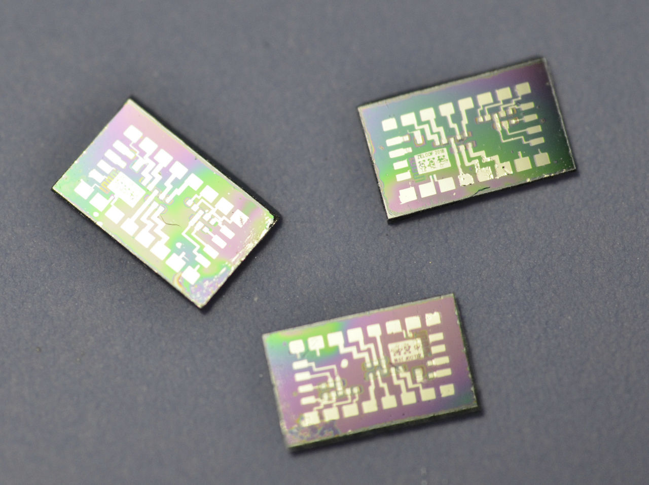
It seems that it is made as designed.
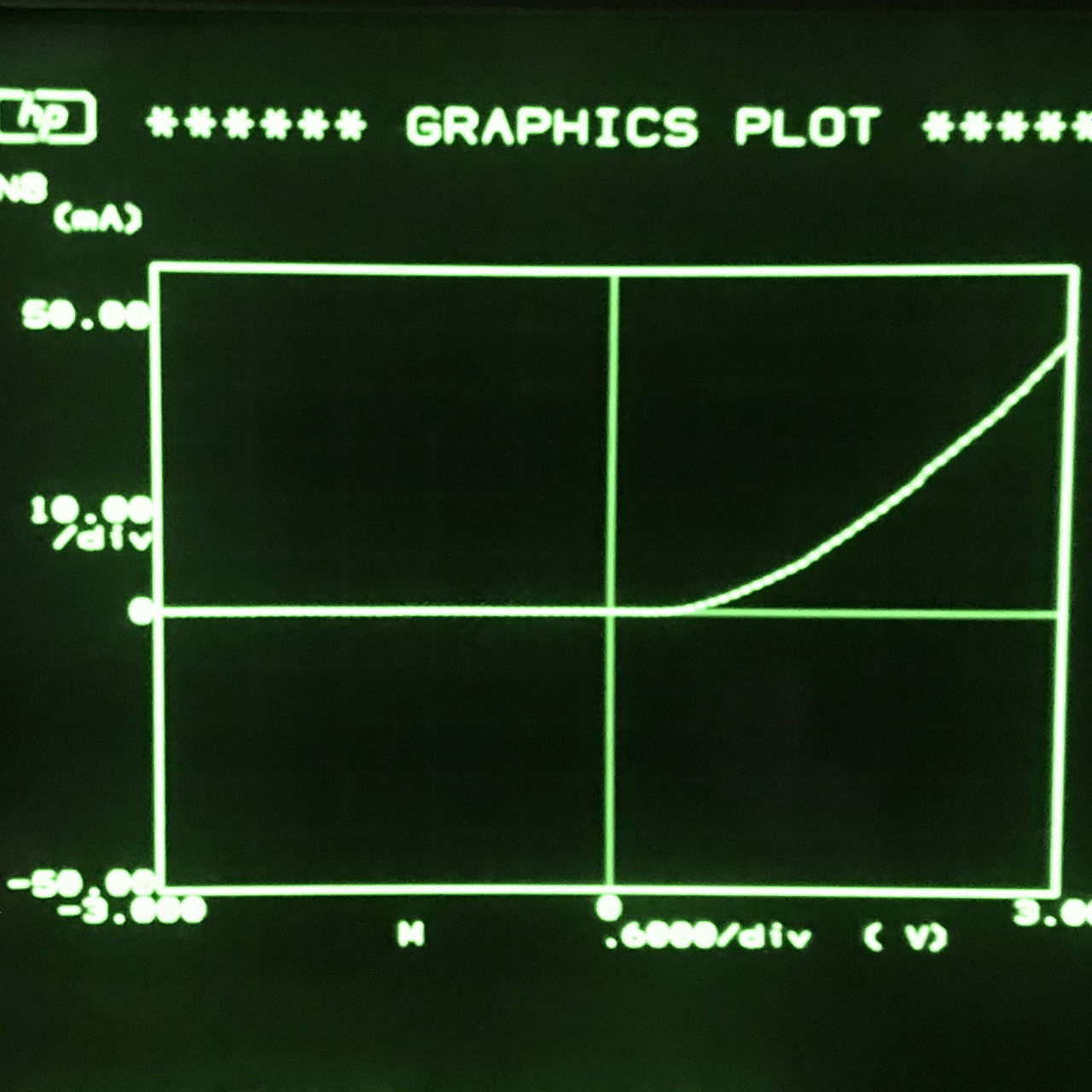
Mr. Zerouf owns no wire bonder, so the test is limited.
Although the Ids / Vds curve of the MOSFET is far from the ideal, it seems that it can be expected to improve if proper wire bonding can be made.
Mr. Zerouf said he was able to learn physics, chemistry, optics, and electricity more than ever by manufacturing IC chips designed by himself. We appreciate the many supporters who cooperated in making IC chips, but I'd like to say that I am fortunate if my own efforts will stimulate others and help the home chip manufacturing revolution.
Related Posts:


in Hardware, Posted by darkhorse_log