Ultrafast optical memory could potentially break through the limits of modern computing speed and power consumption
Photonic computing, which uses light for calculations, has been considered a major obstacle to practical application due to the need to ultimately transfer data processed by light to and from electrical memory. A research team from the USC Information Sciences Institute (USC ISI) and the University of Wisconsin-Madison has proposed the world's first regenerative photonic (optical) memory, which has the potential to overcome the limitations of current computers in terms of processing speed and power consumption, potentially revolutionizing fields such as AI and data centers.
[2503.19544v1] Design of Energy-Efficient Cross-coupled Differential Photonic-SRAM (pSRAM) Bitcell for High-Speed On-Chip Photonic Memory and Compute Systems
Scientists Create Ultra Fast Memory Using Light - Information Sciences Institute
https://www.isi.edu/news/81186/scientists-create-ultra-fast-memory-using-light/
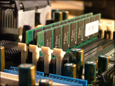
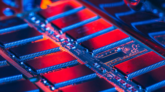
While current computer systems are becoming increasingly miniaturized, resistance and heat generated by the metal wiring that transmits electronic signals are becoming a bottleneck, and it is said that data transfer speeds are reaching their limits. Although the use of optical communication technology has made progress in increasing data transfer speeds, the memory section that stores data still relies on electronic technology.
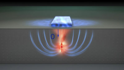
The newly developed photonic SRAM (pSRAM) retains data like conventional electronic memory, but operates using light instead of electricity. It employs a unique cross-coupled microring resonator (MRR) and photodiode structure, enabling data to be written and read using optical signals.
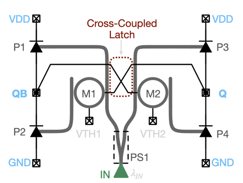
Simulations conducted by the research team showed that pSRAM could achieve extremely fast read and write cycles of 40 GHz. It also demonstrated very high energy efficiency, with switching energy per bit of approximately 0.6 picojoules and static energy during standby of approximately 0.03 picojoules. The bit cell size is approximately 330 x 290 micrometers, which allows for integration into large-scale memory arrays, the research team said.
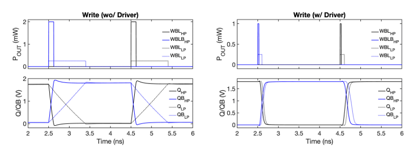
The following is a simulated waveform demonstrating how data in pSRAM can be accurately rewritten using an optical signal. The top graph shows the 'light pulse input' required for writing, while the bottom graph shows how the stored data (voltage Q/QB) flips from '0' to '1' or '1' to '0' upon receiving that light. The graph on the right shows that by combining the drive circuit, data can be successfully rewritten in just 25 picoseconds.
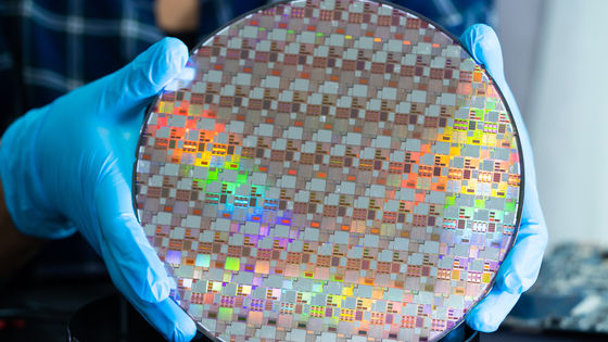
Furthermore, while previous optical memories often required exotic materials, the pSRAM developed here is expected to be manufactured on an existing commercial platform, GlobalFoundries ' 45nm silicon photonics process, which means that it will be realistic to mass-produce large-scale optical memory systems and integrate them with existing electronic systems in the future, the research team argued.
'To fully realize the capabilities of AI accelerators and other devices, optical memory that is just as robust as electrical memory is essential,' said Ajay P. Jacob of USC ISI, who led the research team. The results of this research are scheduled to be presented at the International Electron Devices Meeting (IEDM) in San Francisco in December 2025.
Related Posts: