Intel reveals that it is designing a processor with ``8 cores 528 threads''
At
Intel Shows 8 Core 528 Thread Processor with Silicon Photonics
https://www.servethehome.com/intel-shows-8-core-528-thread-processor-with-silicon-photonics/
Intel Discloses 8 Core & 528 Thread CPU Based on RISC Architecture, 66 Threads Per Core
https://wccftech.com/intel-discloses-8-core-528-thread-cpu-based-on-risc-architecture-66-threads-per-core/
Intel held a session at Hot Chips 2023 titled 'The First Direct Mesh-to-Mesh Photonic Fabric.'
In this session, Intel mentioned the joint research program `` Hierarchical Identify Verify & Exploit (HIVE) '' that was being jointly promoted by the U.S. Department of Defense's Defense Advanced Research Projects Agency (DARPA) and private companies. Announced in 2017, HIVE is a project to improve processors for big data processing, which is essential for machine learning and AI technology, and aims to develop processors that outperform traditional hardware by 1000 times in performance per watt. I did.
Intel, which worked on HIVE, analyzed the workload that DARPA was investigating and discovered that the processing required massive parallelism, and that traditional designs would result in low cache utilization. .
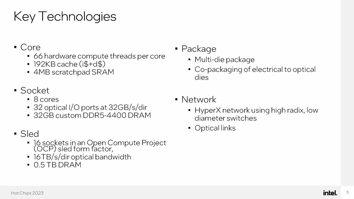
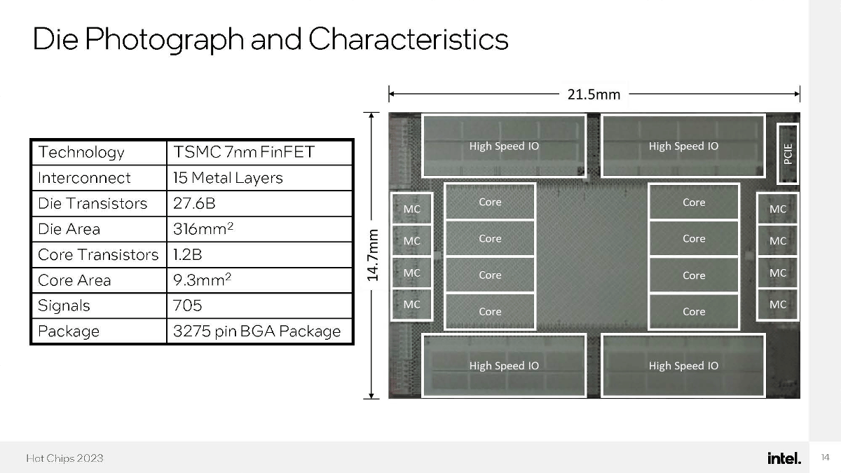
So Intel designed a new processor called an ``8-core processor with 66 threads per core.'' By having a total of 528 threads on one processor, a huge number of tasks can be processed in parallel. Cache memory per core is 192KB and scratchpad memory is 4MB.
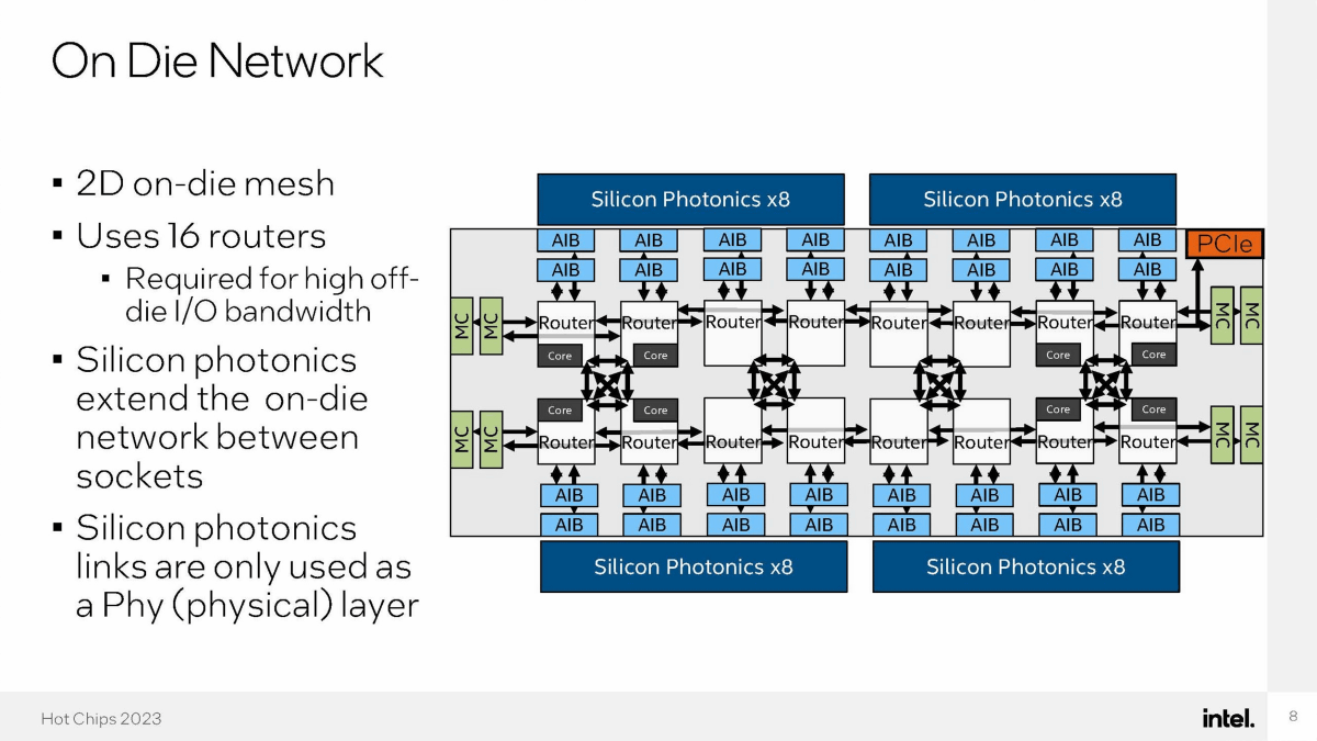
The architecture is
Below is a photo of the actual die manufactured with
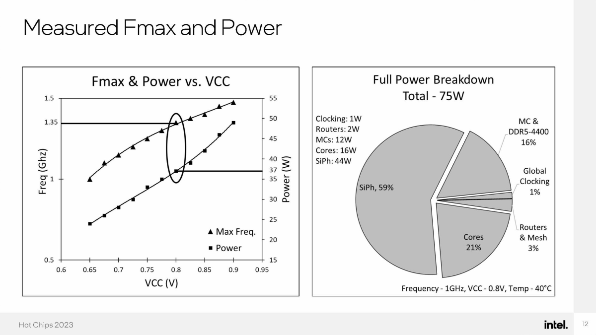
The graph on the right shows the maximum oscillation frequency (Fmax), operating voltage (VCC), and power consumption (Power), and the graph on the left shows the breakdown of power consumption. The thermal design power of this 8-core processor is 75W, of which 59% will be used for silicon photonics.
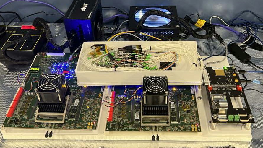
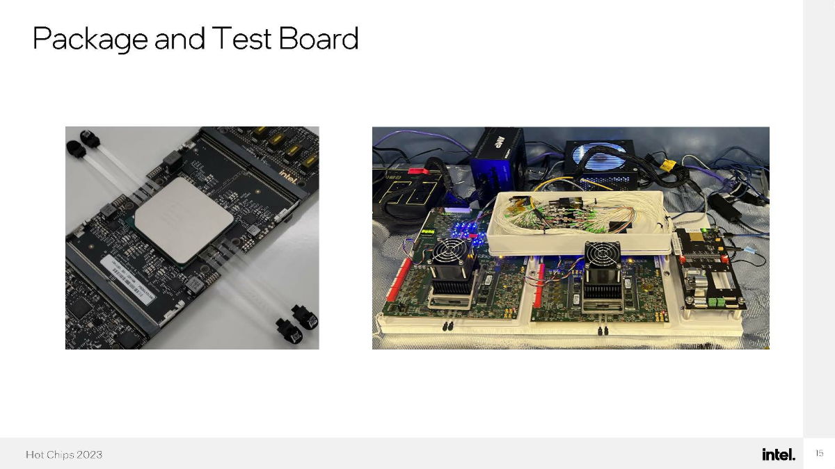
Intel has also published pictures of the actual package and test board.
Related Posts:


in Hardware, Posted by log1h_ik