A fierce man who reverse engineered the Nintendo Switch Lite using 1917 wires appears
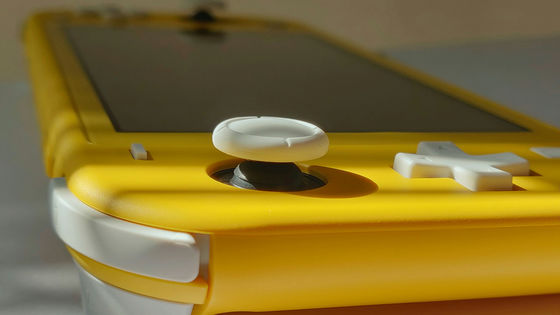
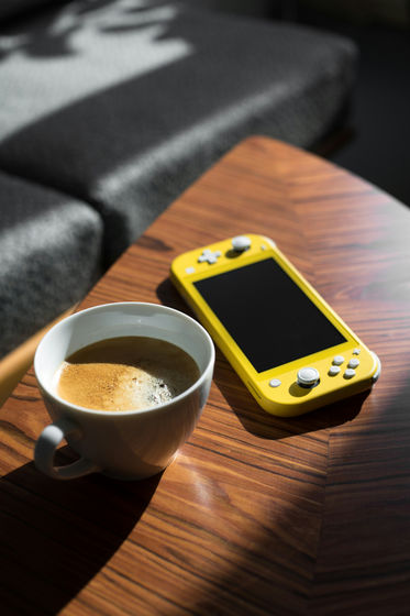
A motherboard is a printed circuit board (PCB) on which wiring, various IC chips, connectors, etc. are mounted. A fierce person who reverse engineered the motherboard of Nintendo Switch Lite using 1917 wires has appeared, and the results have been made public.
Switch Lite Boardview
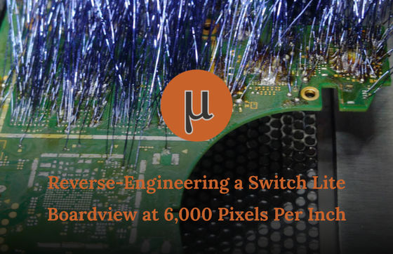
The various components present on the motherboard are soldered to exposed mounting pads, which are connected by copper layers to form electrical circuits. The complete list of where the various components are connected is called a netlist , and when combined with component and pad geometry, becomes the board view. By matching the board view with the reference images of both sides of the PCB, the motherboard output data is completed.
μSoldering, who has over 10 years of experience in the electronics order manufacturing industry that provides services to the medical, aerospace, military, and industrial fields, conducted reverse engineering to create a board view of the Nintendo Switch Lite motherboard. I listed the following three points as points.
1: Process of creating geometric and color accurate panoramic images of assembled PCBs at 6000ppi
2: Point-and-click GUI that can draw geometric parts/pad data on the panorama and also supports adding/changing other arbitrary data.
3: The PCB powers any number of pins one by one, and the state of all pins can be read during each step.
To create a high-resolution image of the motherboard, we desoldered the RF shield on the back of the PCB and took a photo. Import the image into the GUI and record the initial position of parts and pads. After that, it seems that the various components on the motherboard were desoldered and the removed parts were stored separately. μSoldering explains that ultrasonic cleaning was necessary to remove the solder from the RF shield. It seems that many tricks are required to remove the RF shield without using low melting point solder, so in the high resolution image of the completed motherboard, the upper half of the motherboard seems to be dirtier than the lower half.
By recording the binned position and the estimated reference designator in the GUI, we fixed the inconsistency in the 'position information of parts and pads' that was initially created. With all pads exposed and not shorted, connect one lead of a digital multimeter in conduction mode to the ground plane, probe the other lead to any pad on the PCB, and report all hits to the GUI. record.
Using the GUI, group the remaining pads into net fragments based on the visual connections of the two outer board layers. If there are no visible connections, consider the pad to be its own fragment. Then use the GUI to record the order in which wires are soldered from the extractor PCB pins to the target net fragment, assuming they are fragments of the extractor PCB pin itself.
Power travels down wires from the extractor PCB pins into the net fragment, through all hidden connections in the PCB to other net fragments, through those wires back to the extractor PCB, and through all hidden connections in the PCB. It is now possible to create a complete mapping of connected connections. Merge all fragments into the completed netlist based on the extractor mapping.
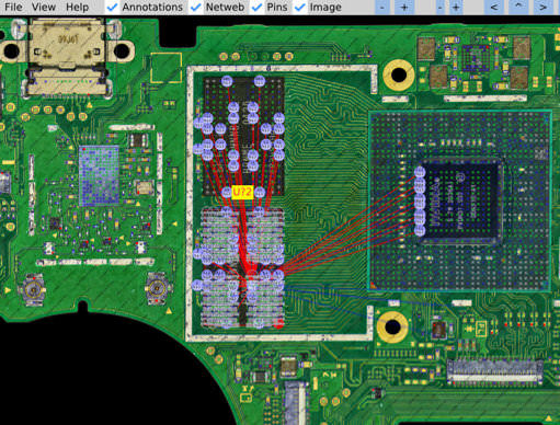
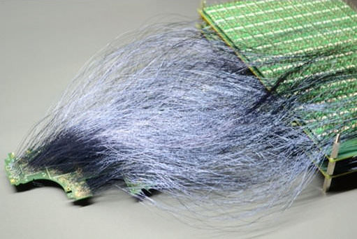
In the end, 2444 photos were used to generate high-resolution images of the front and back sides of the motherboard, and 760 components were desoldered and removed from the motherboard. Masu. The total number of desoldered locations is approximately 30,176, and 1917 wires are used to see how these locations function. It took about three weeks to solder the 1,917 wires, and the entire process took more than a year and cost more than $10,000 (about 1.5 million yen). Masu.
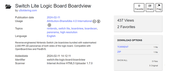
In addition, μSoldering has published the results of his own reverse engineering, and the data can be freely viewed using OpenBoardView , an open source board view software. μSoldering originally said that it would create a panoramic image at 6000ppi, but the version distributed at the link below is 2000ppi. The reason for this is that the data capacity becomes too large, so a 6000ppi version is also distributed separately.
Switch Lite Logic Board Boardview : uSoldering.com : Free Download, Borrow, and Streaming : Internet Archive
https://archive.org/details/switch-lite-logic-board-boardview
Related Posts:
