I designed the board from scratch & soldered the parts to make an original power supply redundancy board
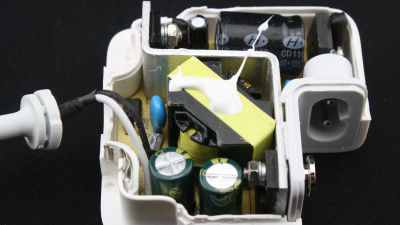
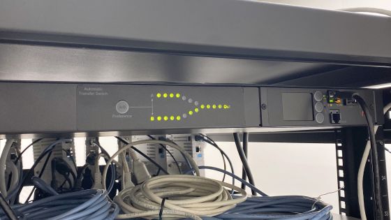
GIGAZINE uses various devices to operate the server, but some of them have only one power system and cannot ensure redundancy. In particular, I want to keep the 'wireless LAN router' that supports the work of the GIGAZINE editorial department always in operation, so I designed an original board and soldered various parts to make a board that can make the power supply redundant. I did.
Since a general wireless LAN router has only one power jack, it will stop due to trouble such as disconnection of the power cable. In order to deal with such troubles, let's make a board that secures power from two systems and combines them into one system.
◆ Board design with KiCad
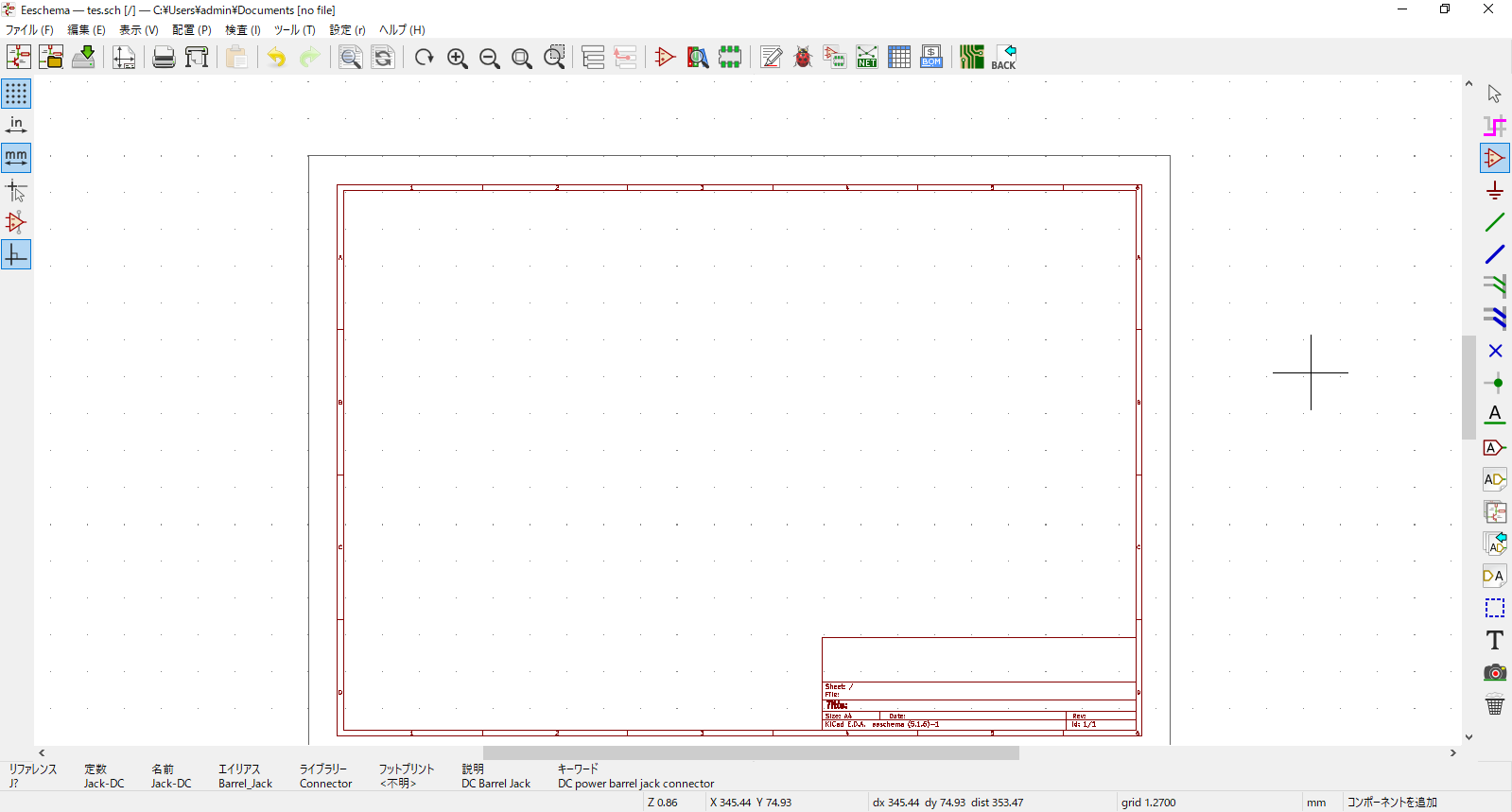
First, we will design the circuit diagram of the board with electronic design software called
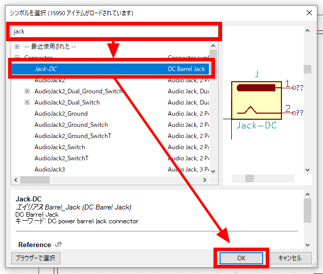
Click the 'Symbols' button on the right bar and click on the schematic to display a window for selecting symbols.

Enter the symbol name of the part you want to use, select the symbol and click 'OK'.
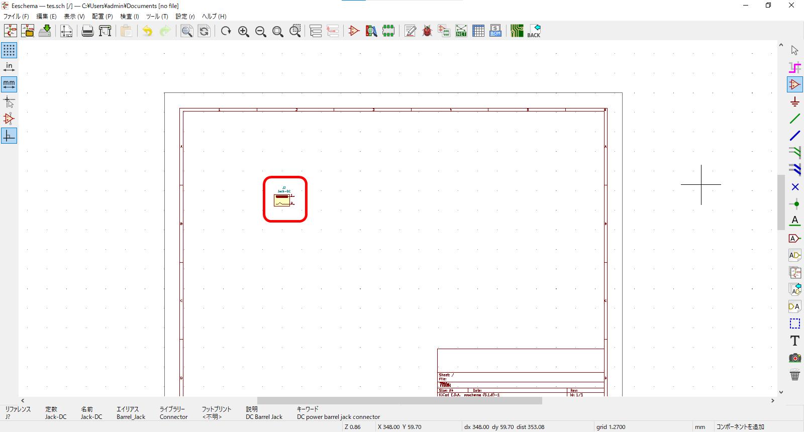
The symbol has been placed. We will place more and more symbols of the parts you want to use like this.
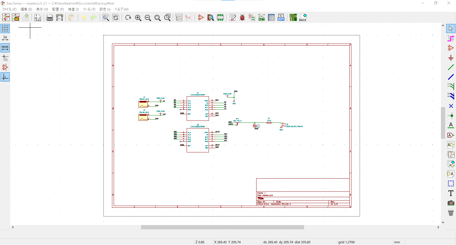
This is the circuit diagram after the symbol placement.
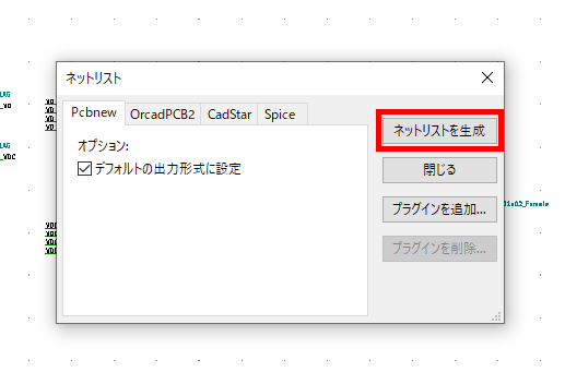
Next, click 'Generate Netlist File' from 'Tools' to output the 'Netlist' for converting symbols to the board layout.
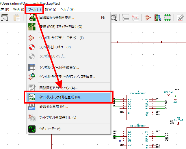
Generate a netlist with 'Generate Netlist'.
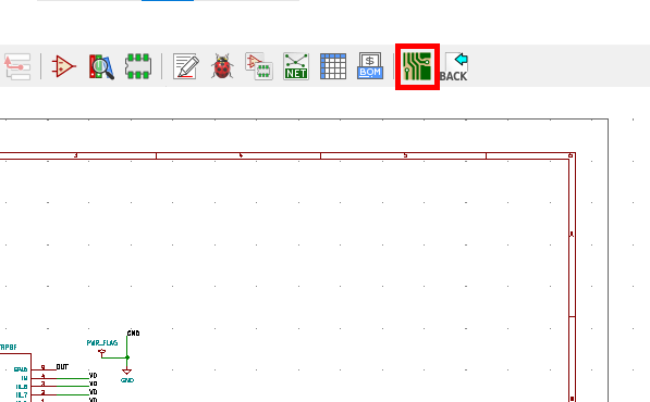
Next, start 'Pcbnew' on the board layout design screen.
After starting Pcbnew, click 'Load Netlist' from 'Tools'.
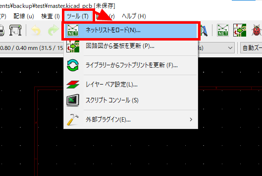
If you specify the netlist output earlier and click 'Update Board' ...
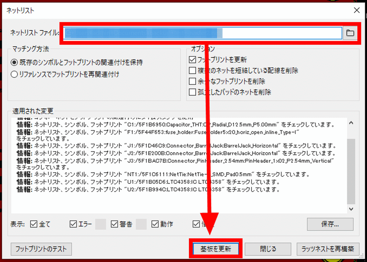
The parts corresponding to the symbols are displayed together.
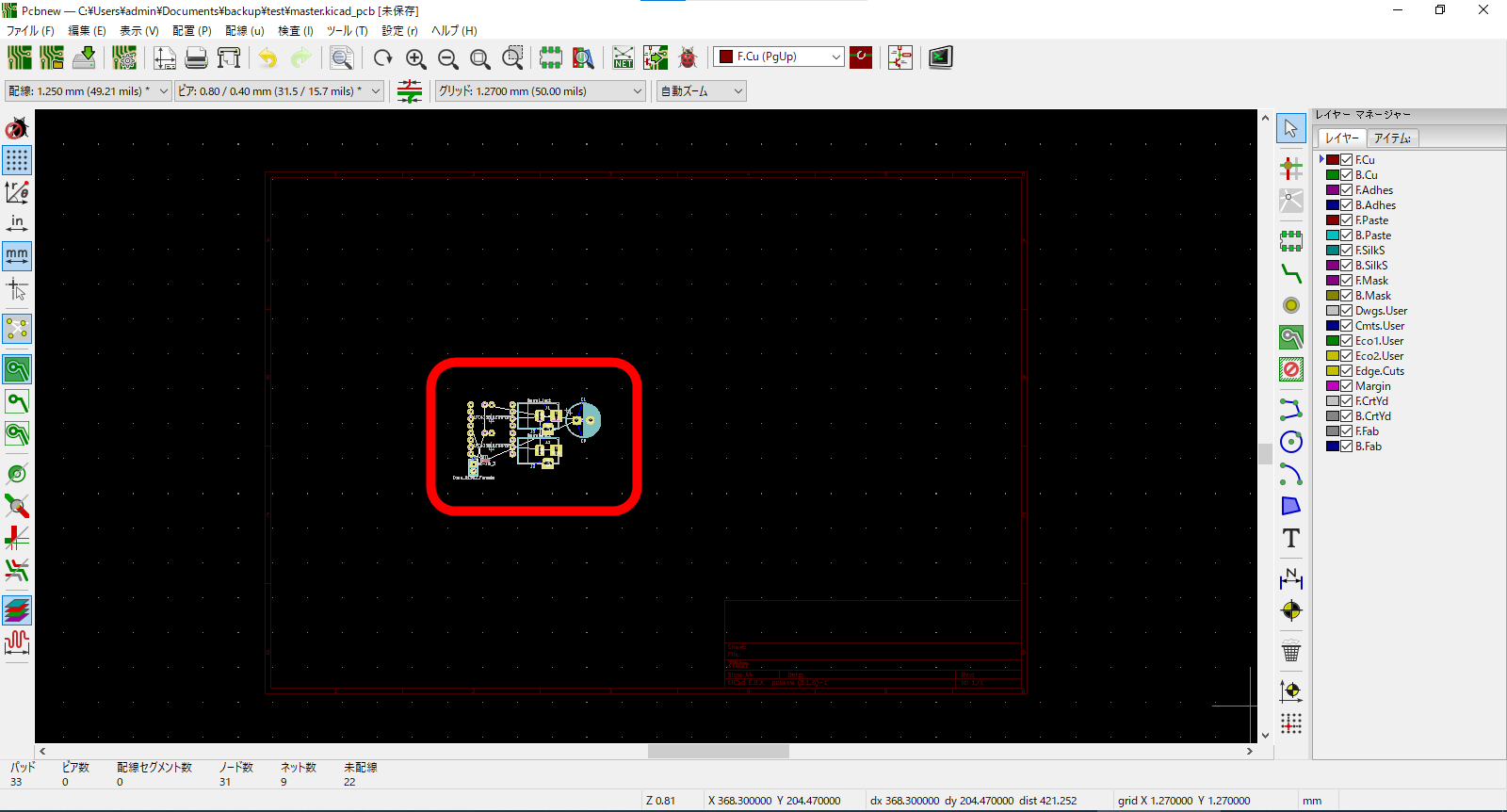
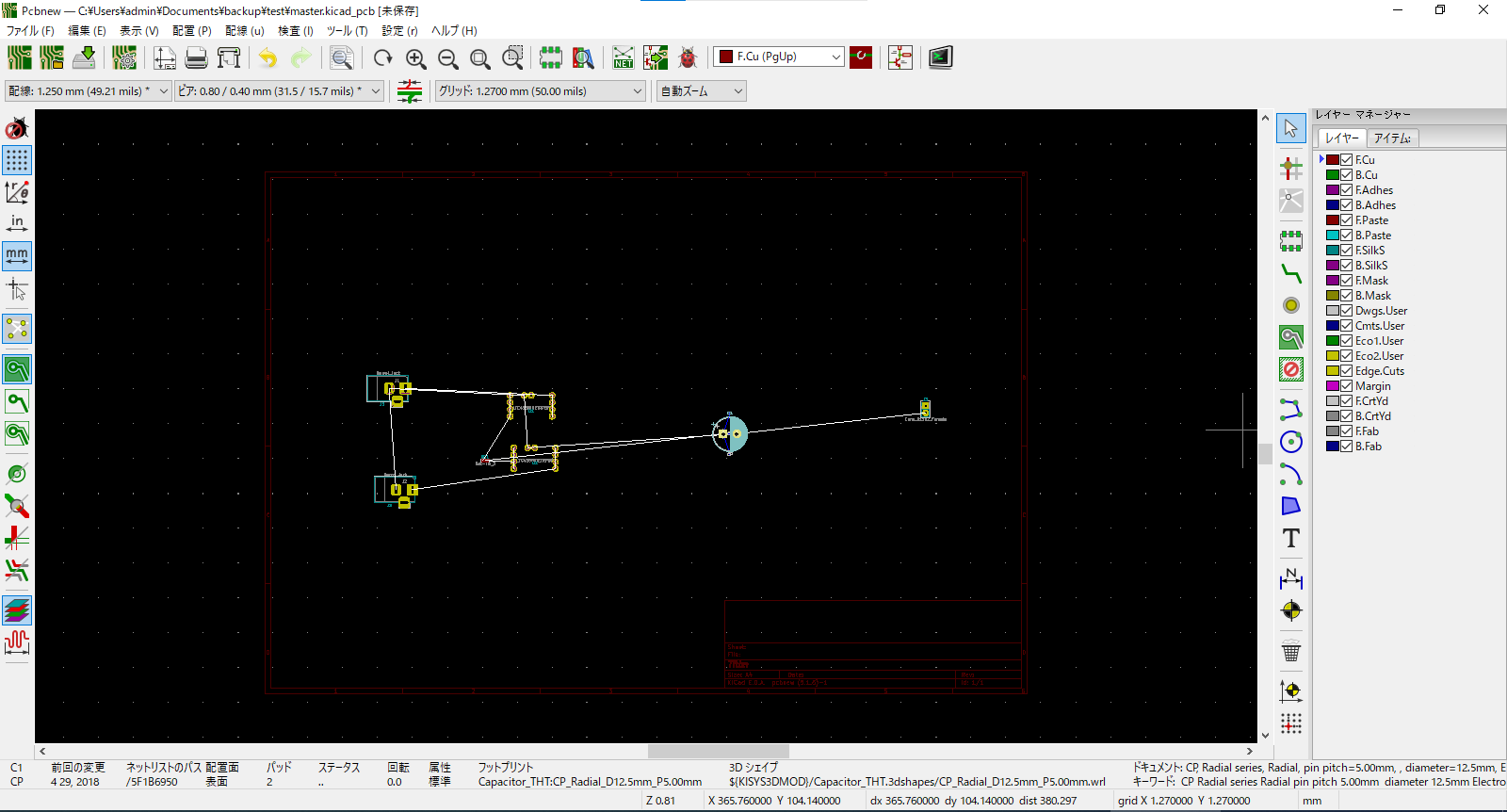
While developing the parts that are output together, we will connect the circuits and design the board layout.
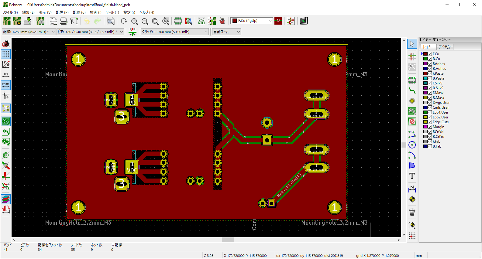
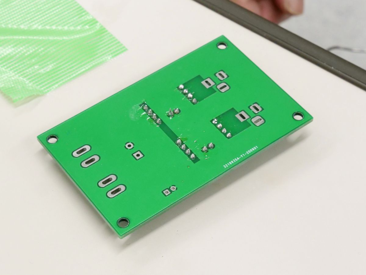
That's why the completed board layout looks like this.
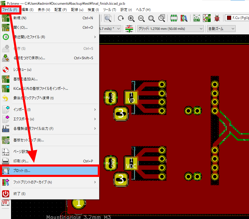
Finally, it outputs the 'Gerber file' required when requesting a board manufacturer. Click 'Plot' from 'File'.
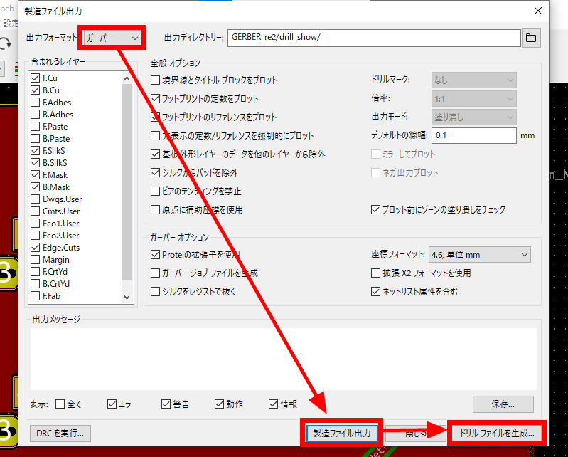
Specify 'Output format' as 'Gerber', click 'Output manufacturing file', and click 'Generate drill file'.
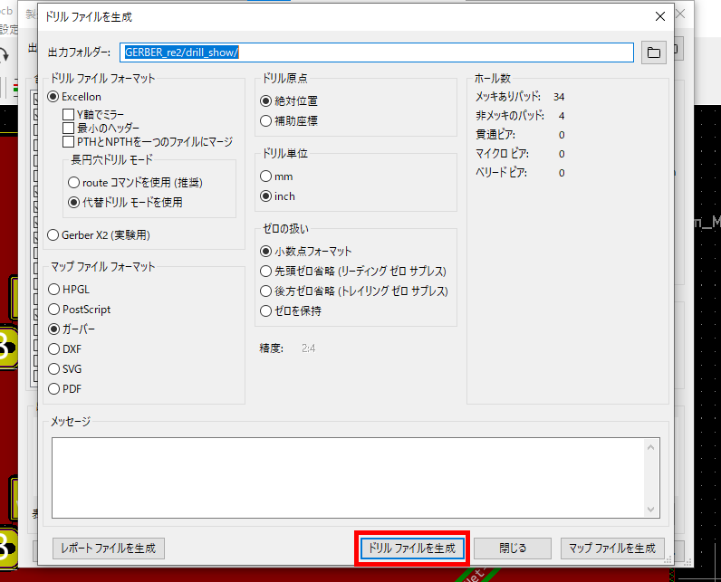
Click 'Generate Drill File' to complete the generation of the Gerber file and the drill file. Submit these files to the vendor and request the board to be manufactured.
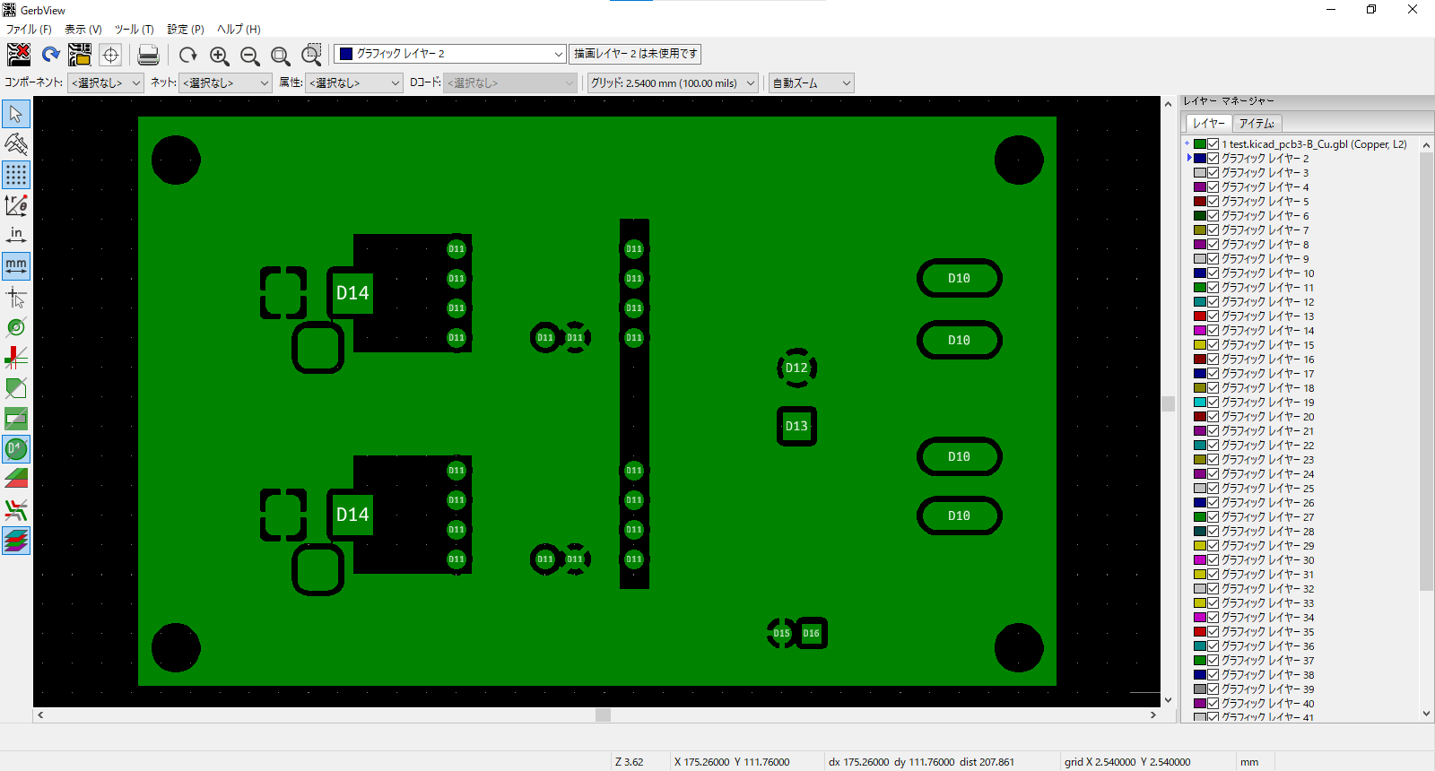
KiCAD also has a function called 'Gerberview' that allows you to preview the Gerber file, so you can use it when you want to check the output result of the Gerber file.
◆ Request JLC PCB to manufacture the board
This time, I decided to ask a company called 'JLCPCB' to manufacture the board.
PCB Prototype & PCB Fabrication Manufacturer --JLCPCB
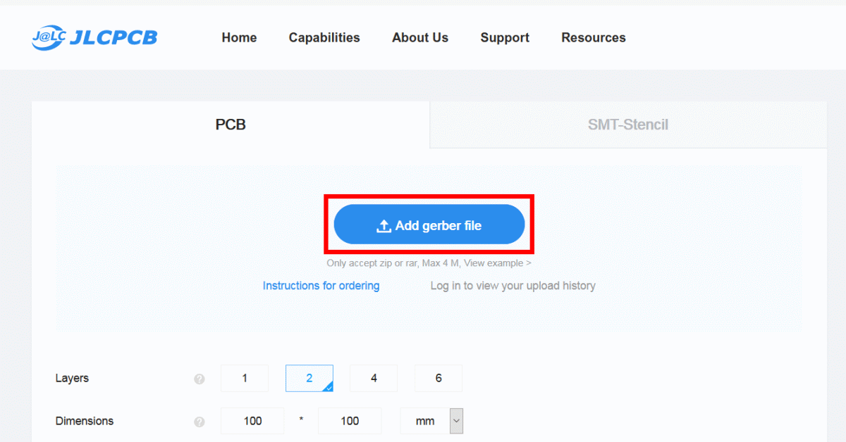
Access the JLCPCB homepage, set the size and quantity of the board, the number of layers, and the thickness of the board, and click 'QUOTE NOW'.

If you upload the gerber file and drill file you created earlier into a ZIP file from 'Add gerber file' ...
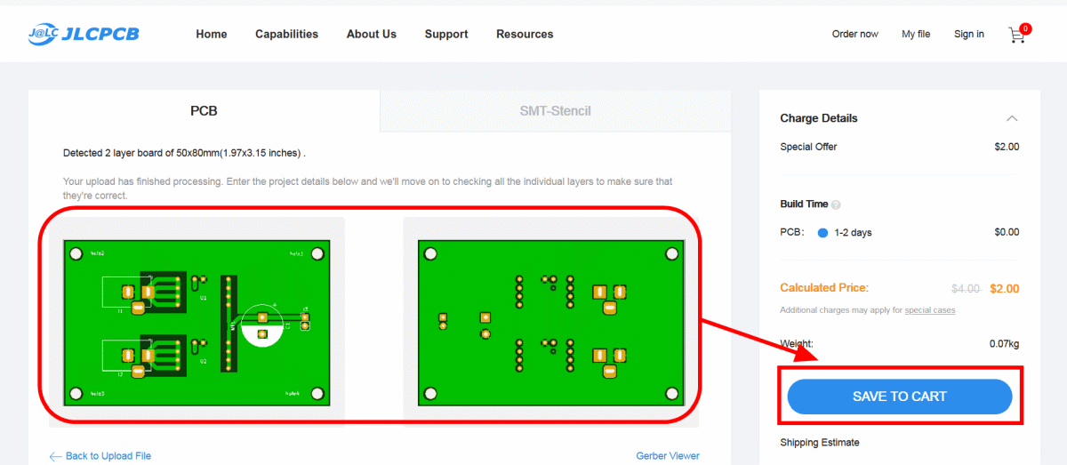
The image of the board is displayed. After that, specify detailed options such as board color and click 'SAVE TO CART'. After completing the payment process, the board production request is complete.
◆ Soldering various parts
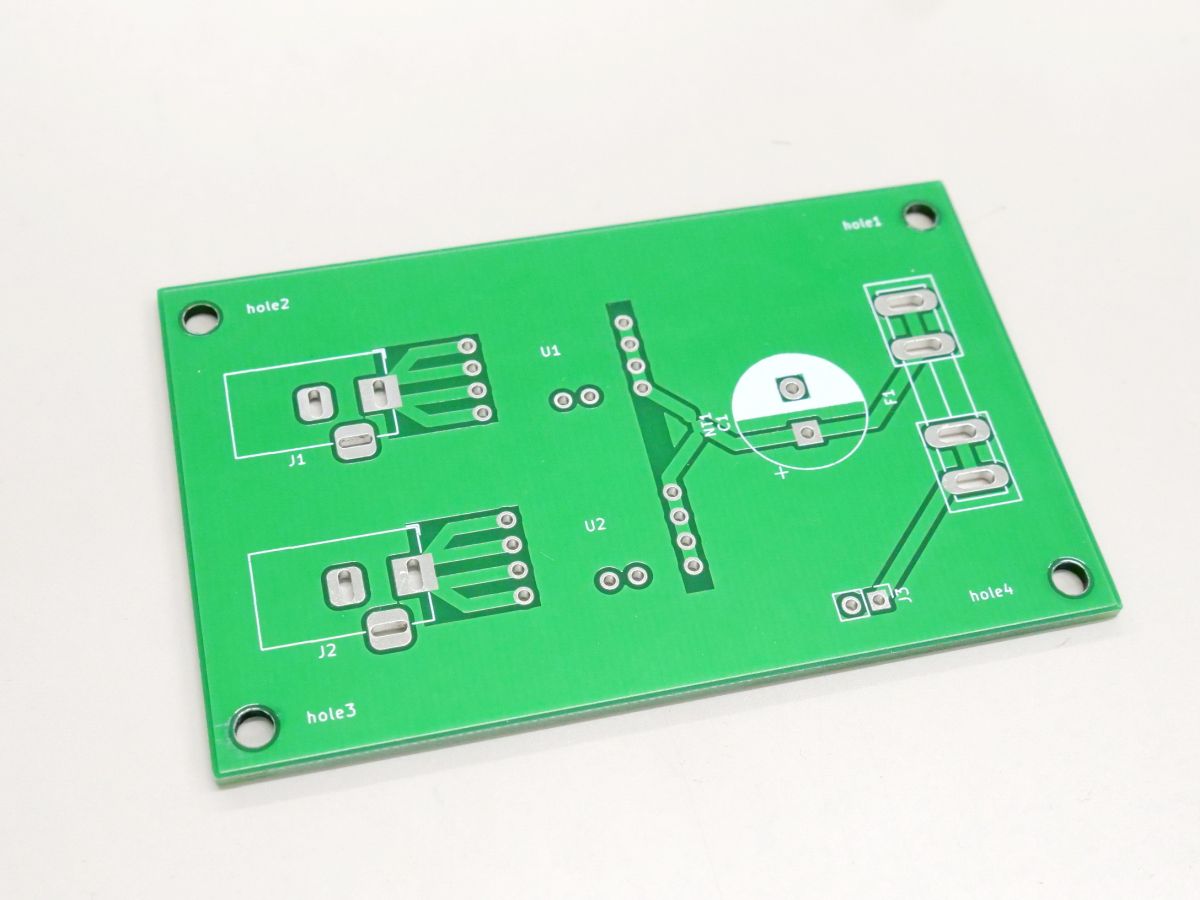
That's why the board arrived in about a week from the request.
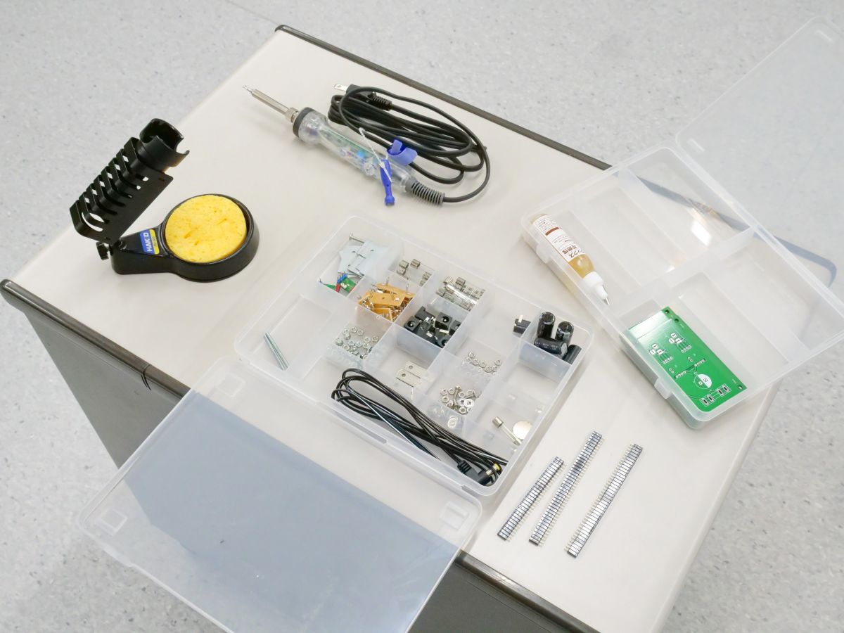
Prepare the soldering iron, solder,
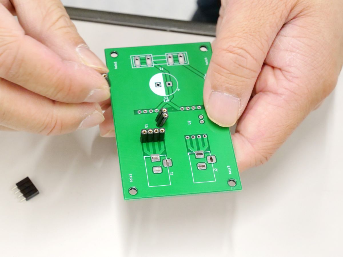
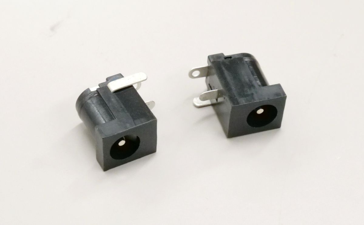
The first thing to attach to the board is the
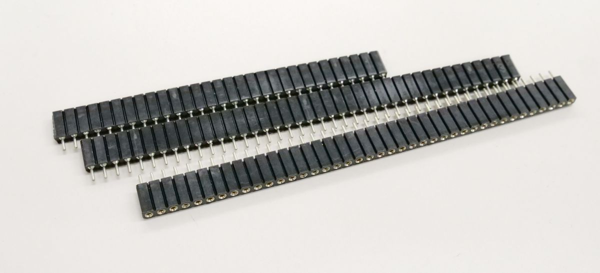
Insert the cut socket into the hole in the board ...
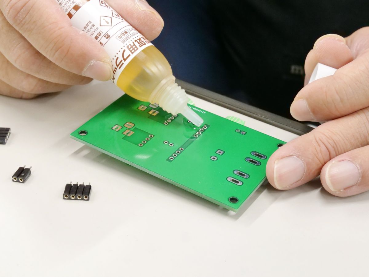
Apply flux to the back side. Flux has the effect of removing foreign matter on the substrate surface and preventing the oxidation of solder. Originally, it should be applied with a brush, but unfortunately there was no brush, so I decided to apply it directly.
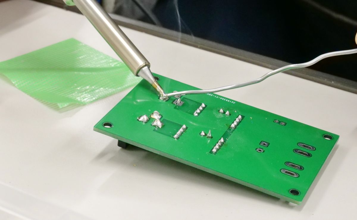
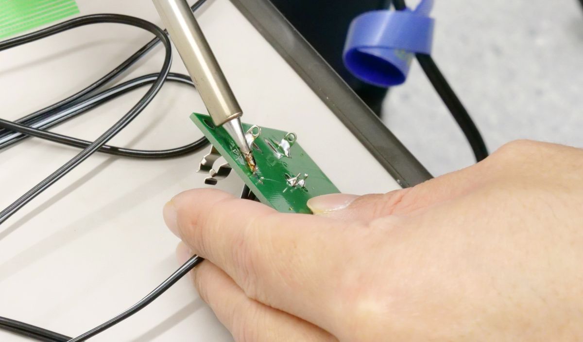
After that, I will solder using a soldering iron.
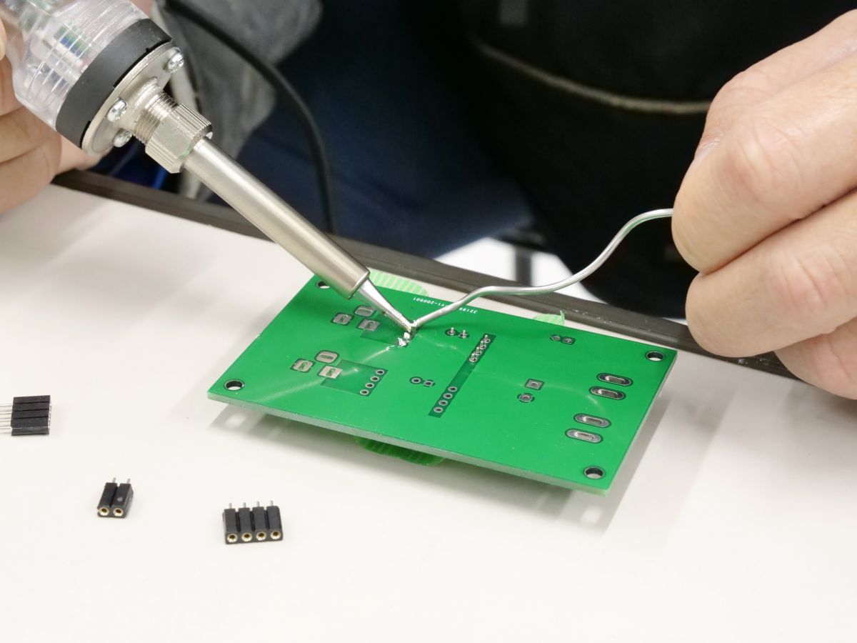
After confirming that adjacent solders do not stick together and cause a 'solder short', socket mounting is complete. The same work will be repeated for subsequent component mounting.
Next to the socket, install two DC power jacks to plug in the power adapter.
This is also coated with flux and soldered.
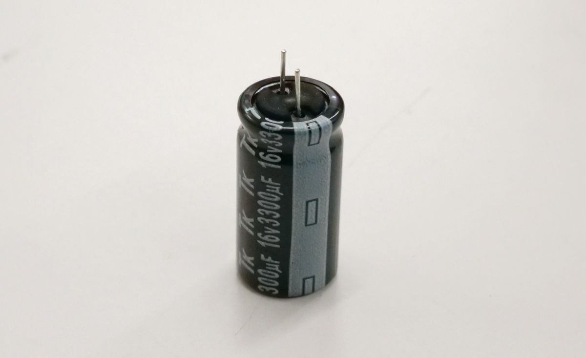
Capacitor to stabilize voltage
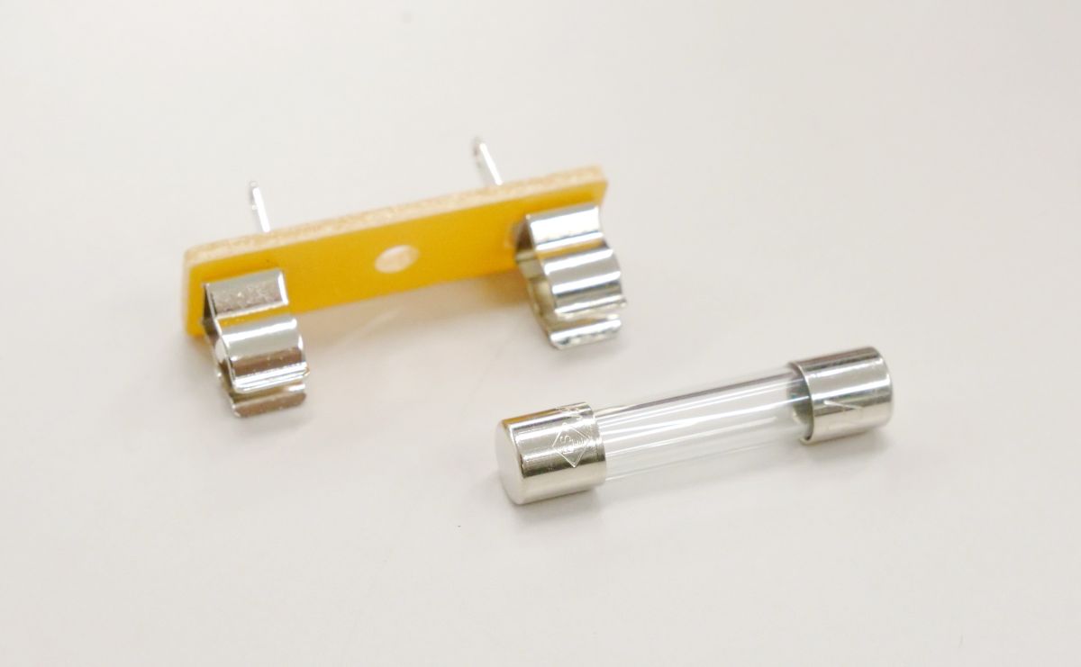
Fuse and fuse box to protect equipment
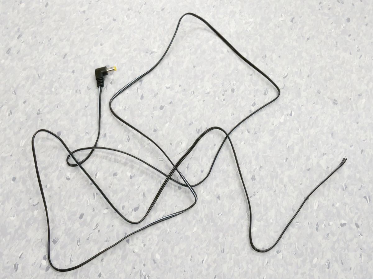
Plug the cable into the power supply of the 'device that wants to make the power supply redundant' ...
Solder firmly.
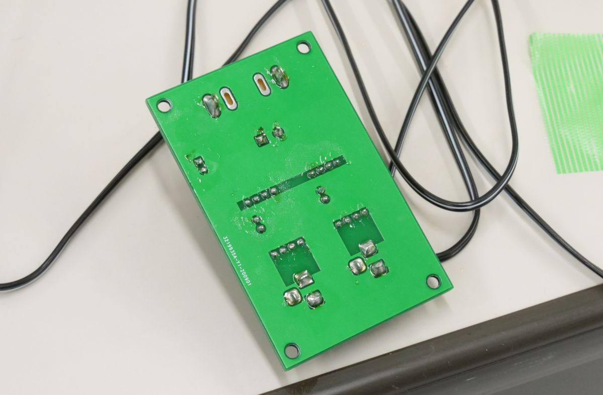
This completes the soldering process.
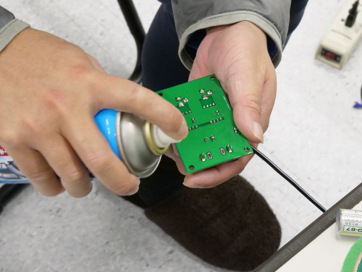
Clean the over-applied flux with a parts cleaner.
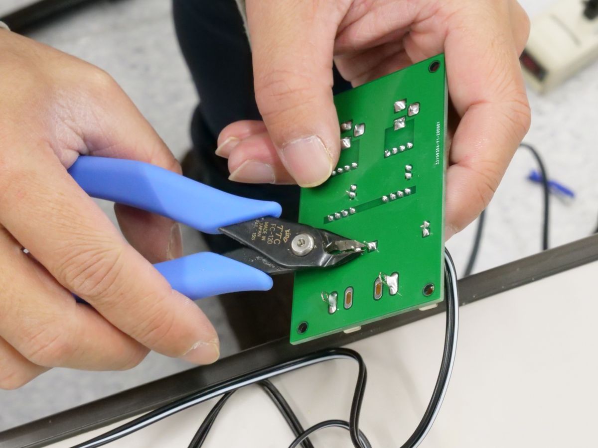
If you cut the pin protruding from the solder with pliers ...
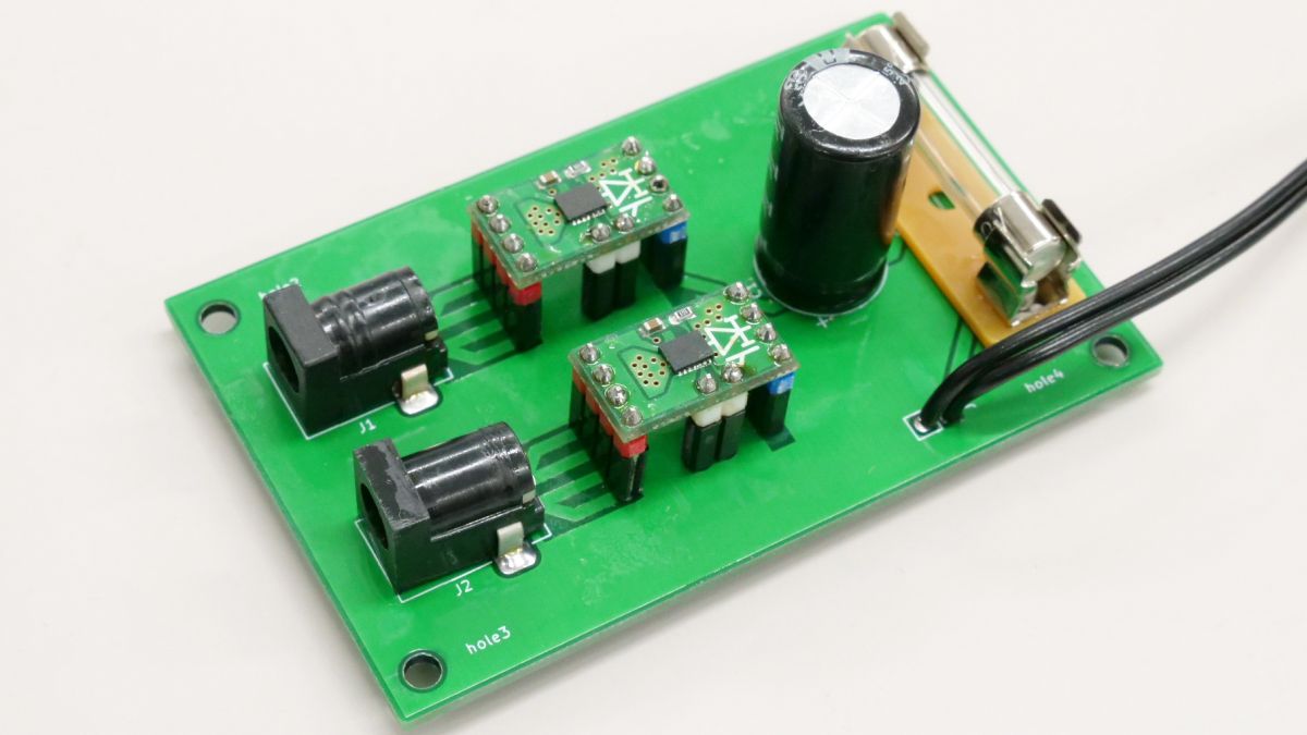
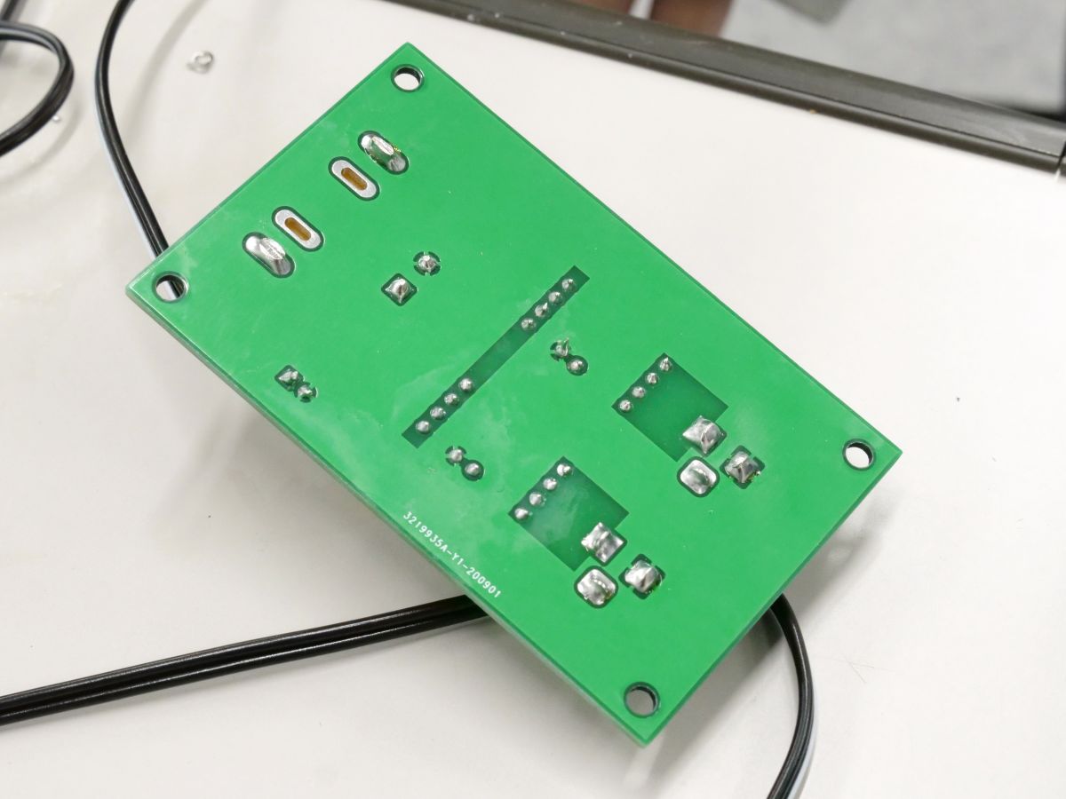
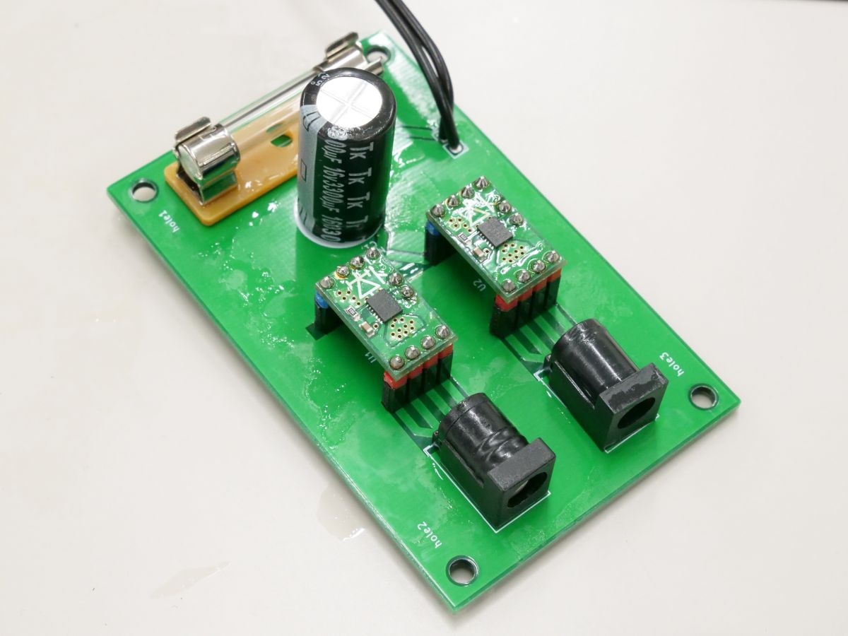
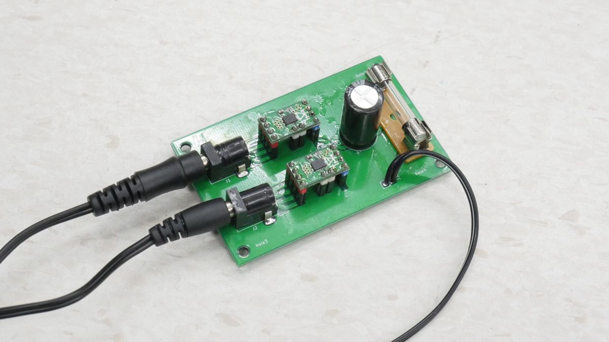
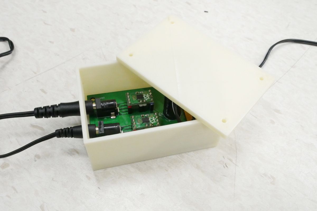
The board body is completed.
Finally, install the '
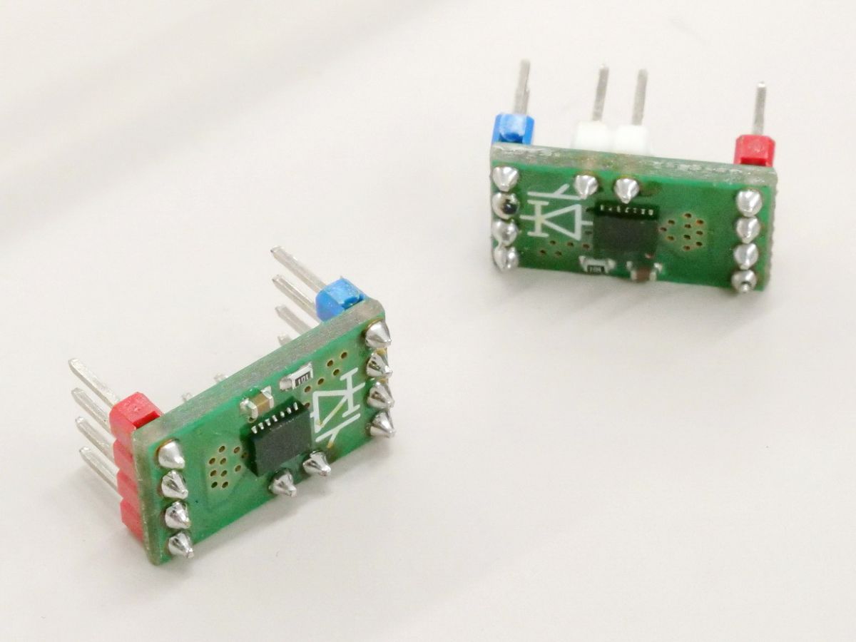
Insert the ideal diode module into the pin socket where it was first mounted, and install a fuse to complete the self-made power supply redundancy board. It is a board that combines the currents input from the two systems into one system while controlling it with an ideal diode so that it does not flow back.
Connect two power adapters ...
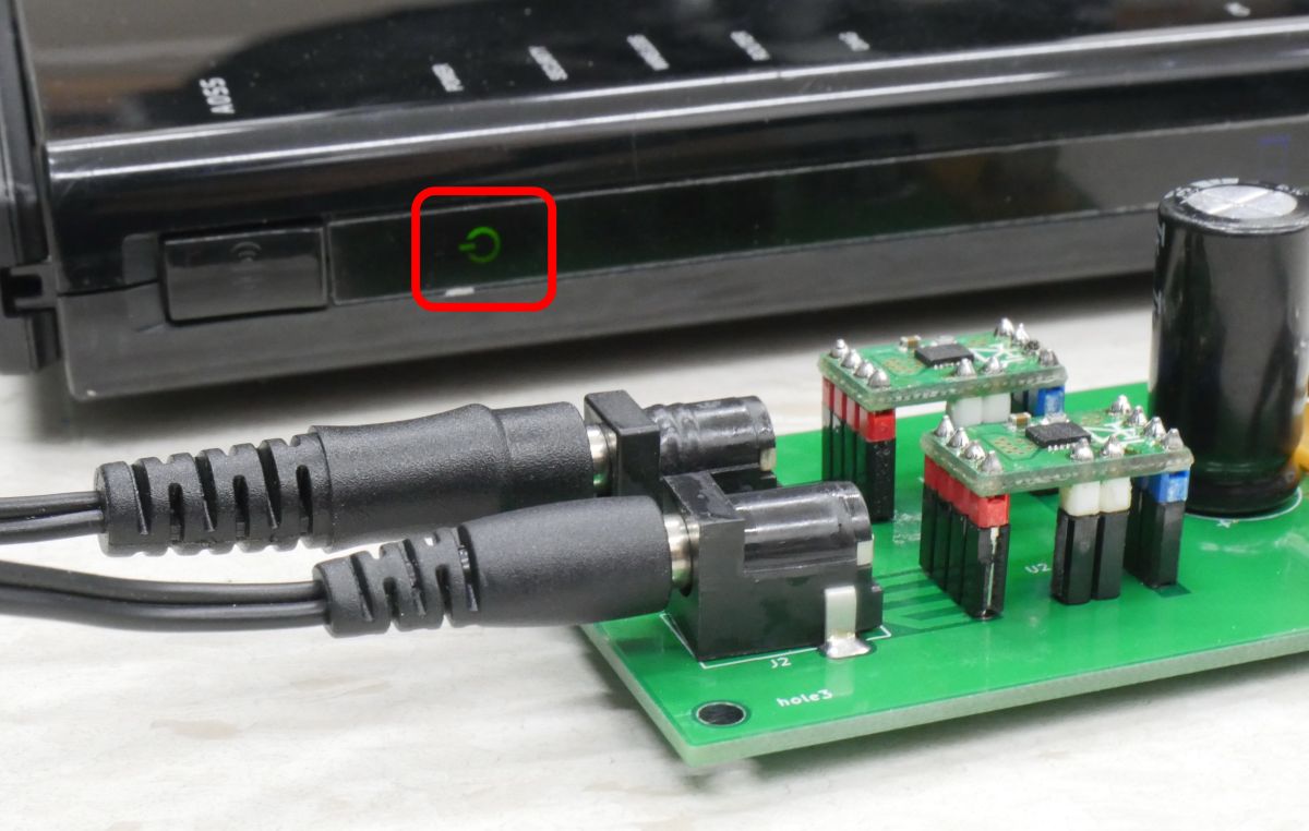
Connect the power cable on the output side to the wireless LAN router.

Naturally, the device will operate normally if the power supply is not turned on.
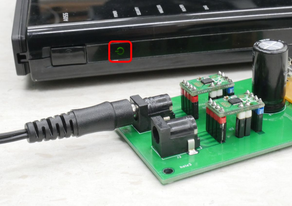
Even if one power supply is removed as shown below, the device remains operating normally. This made it possible to make the power supply redundant even for devices with only one power connector.
You can see how the wireless LAN router works even if the power is plugged in and unplugged in the following movie.
In actual operation, it is used in a case created with a 3D printer.
Related Posts: