NVIDIA announces next-generation 'Ampere' architecture data center GPU 'NVIDIA A100'
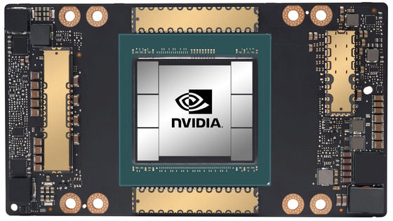
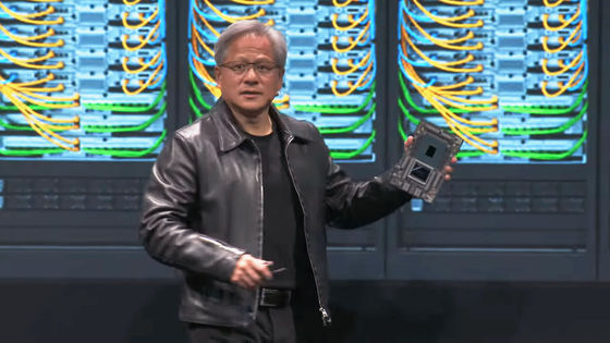
NVIDIA CEO Jenson Huang officially announced the outline of the next-generation 'Ampere' architecture at the keynote speech at the online conference '
DRIVE Platform Moves to NVIDIA Ampere Architecture | NVIDIA Blog
https://blogs.nvidia.com/blog/2020/05/14/drive-platform-nvidia-ampere-architecture/
NVIDIA Ampere Architecture In-Depth | NVIDIA Developer Blog
https://devblogs.nvidia.com/nvidia-ampere-architecture-in-depth/
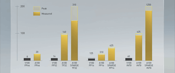
CEO Fan said, “The strong trends in cloud computing and AI are driving structural changes in data center design. With the Ampere microarchitecture, the NVIDIA A100 is a pre-model from data analysis to training to reasoning. It's an end-to-end machine learning accelerator that accelerates AI performance by up to 20 times that of the Tesla V100 . '
In addition, with the third-generation NVLink interconnection implemented on the A100 GPU, the number of links per GPU and switch increases, so the third-generation NVLink significantly expands the communication bandwidth between GPU and GPU, and 50 Gbps per signal pair. It will be possible to transmit the data and improve the error detection and recovery function.
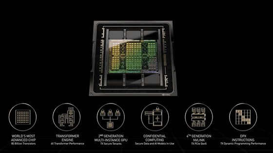
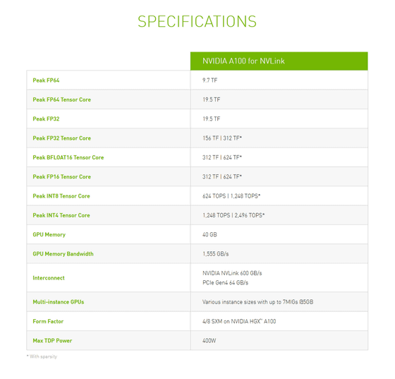
The specific specifications of NVIDIA A100 are as follows. Manufactured by TSMC in the 7nm process, the die size is 826mm 2 , and the number of transistors is 54.2 billion, almost double that of Tesla V100. The GPU memory is 40GB, and the memory bandwidth is 1.555GB / s. Thermal design power is up to 400W.
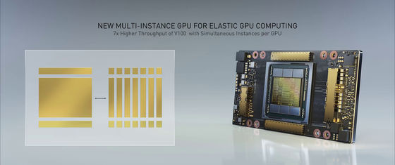
A particularly big feature of A100 GPU is that it includes multi-instance GPU (MIG) function, so-called GPU partitioning function. It is possible to divide GPU resources and process different instances in parallel. One chip can handle up to 7 instances.
NVIDIA's parallel computing platform,
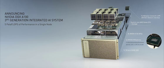
In addition, as a '3rd generation integrated AI system', NVIDIA has 8 A100 for GPU, 2 AMD EPYC Roma for CPU, 15 TB SSD for storage, 6 NVSwitch for switch chip, Mellanox ConnectX for network interface. -The unit 'DGX A100' equipped with nine 200 Gbps units was also announced. According to NVIDIA, the DGX A100 seems to show a computing capacity of 5 peta FLOPS in one unit, and the price will be $ 199,000 (about 21 million yen) per unit.
NVIDIA says the A100 GPU is already in use by various companies and laboratories. According to Microsoft's Vice President Mikhail Parakin, Microsoft has trained the world's largest language model ' Turing NLG ' with 17 billion parameters using NVIDIA GPU of Ampere architecture. `` We will train thousands of NVIDIA's new generation A100 GPUs to dramatically improve AI models on Azure to push the cutting edge of language, voice, vision and multimodality, '' Parakin commented. ..
You can see the keynote speech by CEO Fan in the following movie. Fan CEO is giving the keynote speech at his home kitchen in California.
NVIDIA GTC 2020 Keynote Part 6: NVIDIA A100 Data Center GPU Based on NVIDIA Ampere Architecture-YouTube
Related Posts:
