Jim Keller's semiconductor manufacturing startup, Fab2, is building a factory to mass-produce small semiconductor fabs.
Atomic Semi, a startup founded by Jim Keller, a semiconductor engineer known for designing Apple's A4 chip and AMD's Zen microarchitecture and CEO of AI chip development startup Tensorrent, and Sam Zeruf, known for his in-house semiconductor manufacturing, has changed its name to Fab2 . Fab2 is developing a small semiconductor manufacturing plant and a 'fab fab' to mass-produce the equipment used inside it, and has also moved its base of operations to Texas.
fab2
@Fab2 fabs fabs, fabs printers
— Jim Keller (@jimkxa) July 4, 2026
Prints on masks, prints on chips
make everything
Atomic Semi is now @fab2 https://t.co/Gno88bWLiU
Jim Keller's startup is building a factory to mass-produce small semiconductor fabs —Atomic Semi rebrands as 'Fab2' underlining intended role as a 'fab fab' | Tom's Hardware
https://www.tomshardware.com/tech-industry/atomic-semi-rebrands-as-fab2-and-shifts-operations-to-texas
Atomic Semi is a semiconductor manufacturing startup founded in 2022. Its founders are Mr. Keller and Mr. Zeruf, who is self-taught in semiconductor manufacturing.
Jim Keller, the genius engineer who created AMD Ryzen and Apple A4, has launched a semiconductor manufacturing company called 'Atomic Semi' - GIGAZINE

Fab2 aims to be a 'fab fab,' a factory that builds the fab itself for semiconductor manufacturing. The plan is to design and manufacture pumps, valves, sensors, gas piping, nanometer-precision actuators, control boards, and other components in-house, assemble them into a single device, and then assemble that manufactured device into a semiconductor fab.
New name, same mission.
— Sam Zeloof (@szeloof) July 4, 2026
Atomic Semi is now Fab2.
Fab2 prints chips and fabs https://t.co/kNJ9invTjR pic.twitter.com/Hx13eAyNPR
The company name change from Atomic Semi to Fab2 clearly indicates its commitment to making 'fab fab' the core of its business. Fab2 aims to mass-produce small fabs by assembling a complete set of manufacturing equipment in-house, explaining that 'we cannot realize our ideal fab with existing parts alone, so we manufacture the components ourselves.'
Instead of processing 300mm wafers on a massive production line, Fab2 envisions using software-defined miniature fabs capable of processing chips smaller than wafers. According to hardware news outlet Tom's Hardware, Fab2 aims to complete prototype chips in just a few hours, positioning speed for prototyping and small-batch production as its main value.
On the other hand, this method has limitations in terms of production volume. For example, because electron beam lithography directly writes patterns without using a mask, it takes longer than when an EUV lithography system exposes an entire 300mm wafer. Therefore, it is considered a method more suitable for prototyping and low-volume applications than for mass production like that of state-of-the-art foundries.
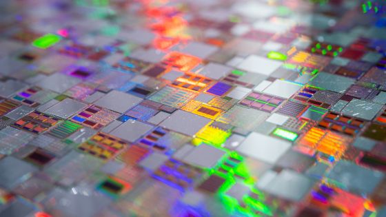
wafer inspection pic.twitter.com/Af5mKkpRIn
— Fab2 (@fab2) February 12, 2024
Fab2 develops not only manufacturing equipment but also chip design software called 'Studio.' Studio is a collaborative EDA tool that runs in a browser and supports layout, schematics, and simulations. Fab2 aims to support the operation of small-scale fabs by accelerating not only manufacturing equipment but also the design process.
The company has three locations: Austin and Lockhart in Texas, and San Francisco in California. In Austin, it has a facility totaling approximately 120,000 square feet for research and development and production, while in Lockhart, it operates a 'fab-fab' facility totaling approximately 30,000 square feet. In San Francisco, there is also a 'garage-fab' facility totaling approximately 25,000 square feet.

While the existing semiconductor industry concentrates capital investment on massive factories, Fab2 is taking a different approach by deploying numerous small, replicable fabs. The success of its practical application depends on its ability to meet productivity, manufacturing costs, and customer-required process technologies, but it is attracting attention as an initiative to mass-produce semiconductor manufacturing equipment itself.
Related Posts:
in Hardware, Posted by log1i_yk