IBM announces world-first 0.7nm node chip technology, nearly doubling transistor density with its 3D structure 'nanostack'.
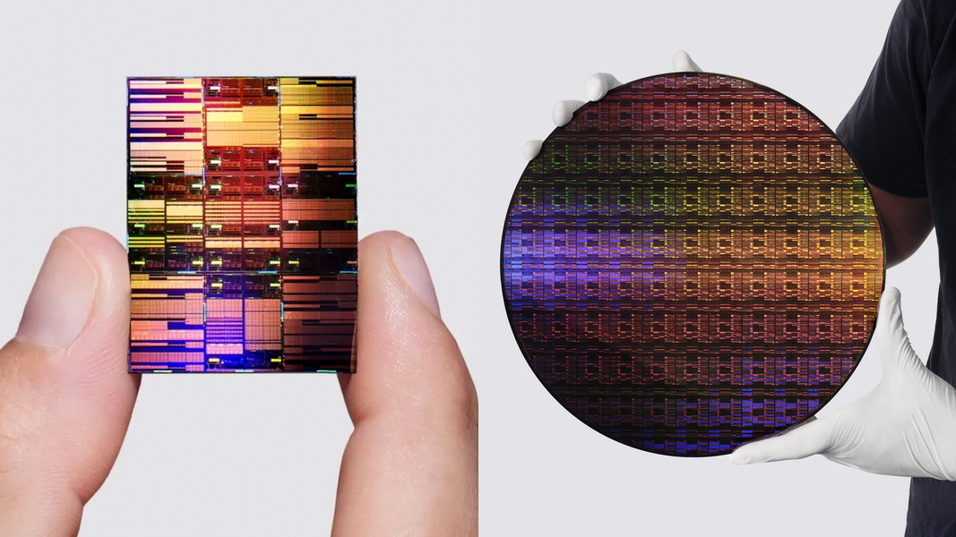
IBM announced on June 25, 2026, the world's first 0.7nm, 7Å (angstrom) node chip technology. Based on a three-dimensional transistor architecture called ' nanostack ,' IBM positions this technology as a foundational technology that will enhance the performance and efficiency of computers, consumer electronics, communication equipment, transportation systems, and critical infrastructure as semiconductor miniaturization approaches its physical limits.
IBM introduces the smallest computer chip in the world - IBM Research
IBM Debuts World's First Sub-1 Nanometer Chip Technology
https://newsroom.ibm.com/2026-06-25-ibm-debuts-worlds-first-sub-1-nanometer-chip-technology
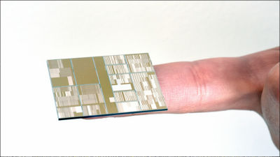
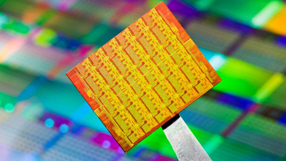
IBM's 7Å, or 0.7nm node, chip integrates approximately 100 billion transistors on a chip about the size of a fingernail. This new chip will have nearly double the transistor density of the 2nm node chip announced in 2021.
IBM explains that multiple innovations in structure and materials have demonstrated the potential to improve performance and energy efficiency even in regions where chip components approach atomic size. According to IBM, 0.7nm node chip technology is expected to achieve up to 50% higher performance or 70% higher energy efficiency compared to 2nm node chips, which is anticipated to expand computing power and reduce power consumption in generative AI, cloud infrastructure, and next-generation electronic devices.
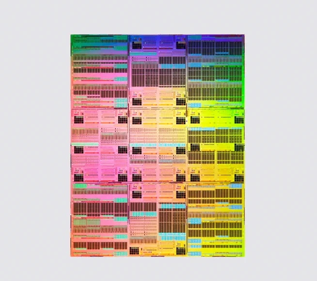
The underlying nanostack is the industry's first 3D transistor structure based on nanosheets. Nanosheets were developed by IBM and have become one of the main design technologies used in advanced semiconductors. nanostack uses 3D sequential integration, which stacks transistors vertically and shifts their position, allowing more transistors to fit into the same area.
Each layer in the stacked structure can employ a different combination of materials, allowing for individual optimization of the performance and power consumption of each transistor. IBM validated nanostack through ultrathin dielectric junctions in CMOS integration, techniques for designing two types of channels, and the actual operation of a CMOS inverter. The validation results demonstrate that nanostack is physically manufacturable and capable of handling actual computing tasks.
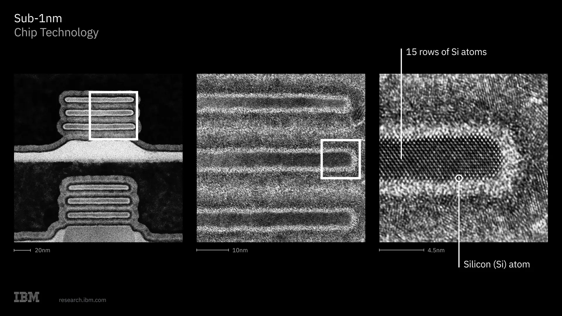
Jay Gambetta, Director of IBM Research and IBM Fellow, commented, 'With the nanostack architecture, we're not just miniaturizing transistors; we're reinventing how chips are built, significantly improving processing performance and energy efficiency.'
At
The node names, such as 0.7nm and 7Å, do not refer to the precise dimensions of the internal structure of the chip, but rather to the generation of the manufacturing technology. IBM claims that nanostack will enable the first-ever extension of logic semiconductors to sub-1nm nodes. IBM's semiconductor roadmap anticipates continued miniaturization using nanostack for at least 10 years, and IBM stated that it has a path to production as early as the next five years. IBM does not manufacture semiconductors for mass production in-house, and has not disclosed any partner companies that will commercialize this technology.
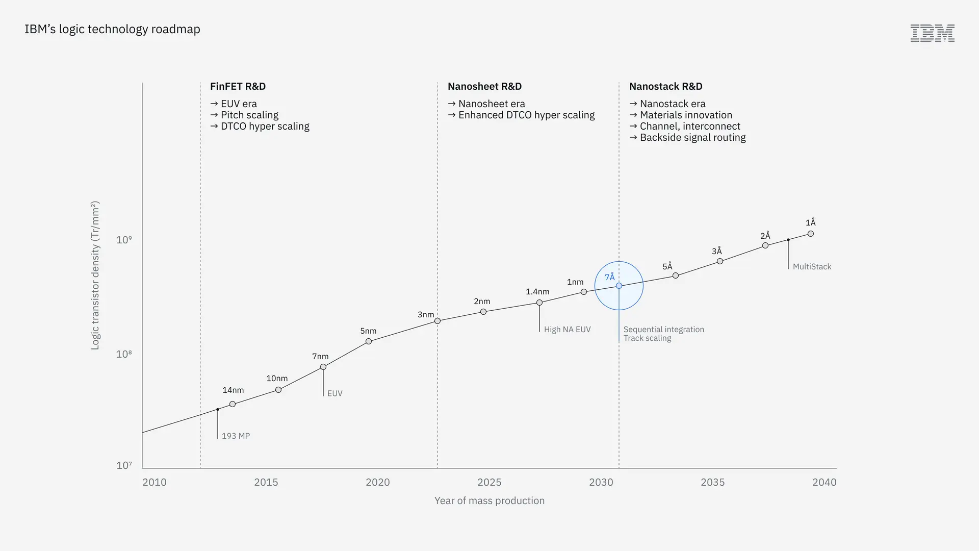
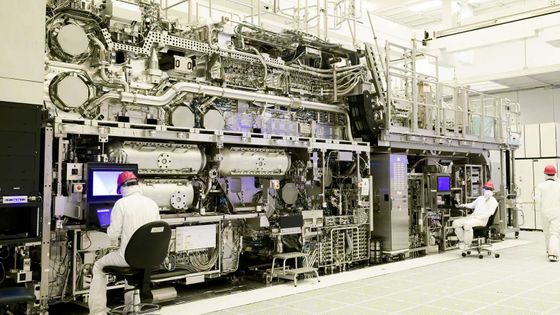
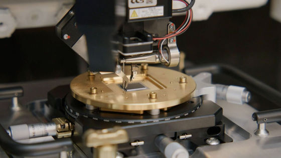
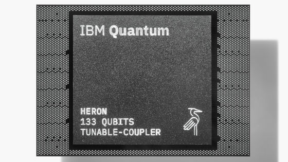
IBM and its partners are conducting research at a semiconductor research facility in Albany, New York. This facility is slated to be equipped with ASML's next-generation High NA EUV (High Numerical Aperture Extreme Ultraviolet) lithography system. Furthermore, IBM is collaborating with companies such as Lam Research , Tokyo Electron , and SCREEN Semiconductor Solutions to jointly develop processes and equipment for High NA EUV, and has already demonstrated working devices. IBM has also announced plans to establish Anderon, the world's first quantum-dedicated foundry, as an independent business entity.
Related Posts:

in Hardware, Posted by log1i_yk