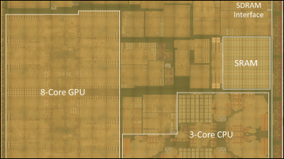
How are semiconductor chip grades determined, and how can we increase production of high-grade products?
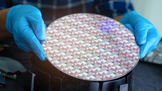
Cerebras, a company that develops semiconductor chips for AI that claim to be '
the fastest AI chips on the planet ,' explained in a blog post how it has increased the yield of semiconductor chips.
100x Defect Tolerance: How Cerebras Solved the Yield Problem - Cerebras
https://cerebras.ai/blog/100x-defect-tolerance-how-cerebras-solved-the-yield-problem

The manufacturing of semiconductor chips is very delicate, and there is a certain probability of defects occurring. Increasing the size of a semiconductor chip can improve its performance, but there is a trade-off: the probability of containing defective areas increases and the yield drops rapidly. The size of early microprocessors was limited by 'how much yield we wanted to ensure.'
In the 2000s, microprocessors with multiple cores per chip emerged, and by making all cores identical and independent in design, the remaining cores could continue to operate even if one core was defective. Companies such as Intel, NVIDIA, and AMD adopted this 'core-level redundancy' strategy, and for example, Intel's first dual-core design,
the Intel Core Duo , was sold as a single-core product, the Intel Core Solo, when one of the cores was defective.
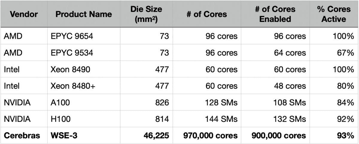
Even today, 'core-level redundancy' is widely used, and it is common for CPUs to be sold with all cores enabled as 'top-of-the-line models' like the EPYC 9654 or Xeon 8490, and with some cores defective as 'budget versions' like the EPYC 9534 or Xeon 8480+. Datacenter GPUs are so large that even the top-of-the-line models have some cores disabled.
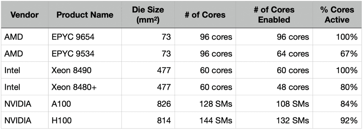
NVIDIA's H100 is a huge GPU with an area of 814 square millimeters, and it is extremely difficult to manufacture it without defects. Therefore, when designing the H100, NVIDIA physically placed 144 SMs (streaming multiprocessors), which are the core management units, and limited the number of SMs actually enabled to 132, so that the product could be sold even if up to 12 SMs had defects.
In the past, semiconductor chips with an area of 814 square millimeters were not economically viable due to yield problems, but at the time of writing, they have become mainstream products by adopting designs that tolerate defects. When a defect occurs, the entire core containing the defect becomes unusable, so Cerebras explains that 'by making the core as small as possible, we can improve defect tolerance.'
In designing semiconductor chips, Cerebras focused on making the core as small as possible, and designed the core to be 0.05 square millimeters in size. This is about 1/100th the core size of the H100, and the area that is disabled when a defect occurs is also about 1/100th, so Cerebras' WSE-3 is effectively 100 times more defect-resistant than the H100.
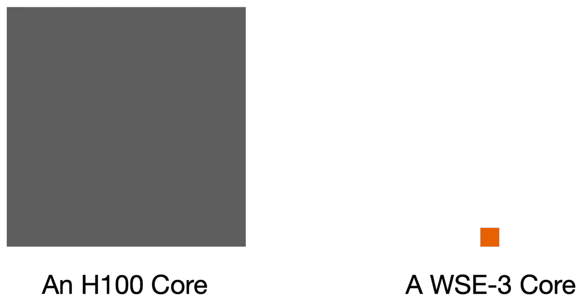
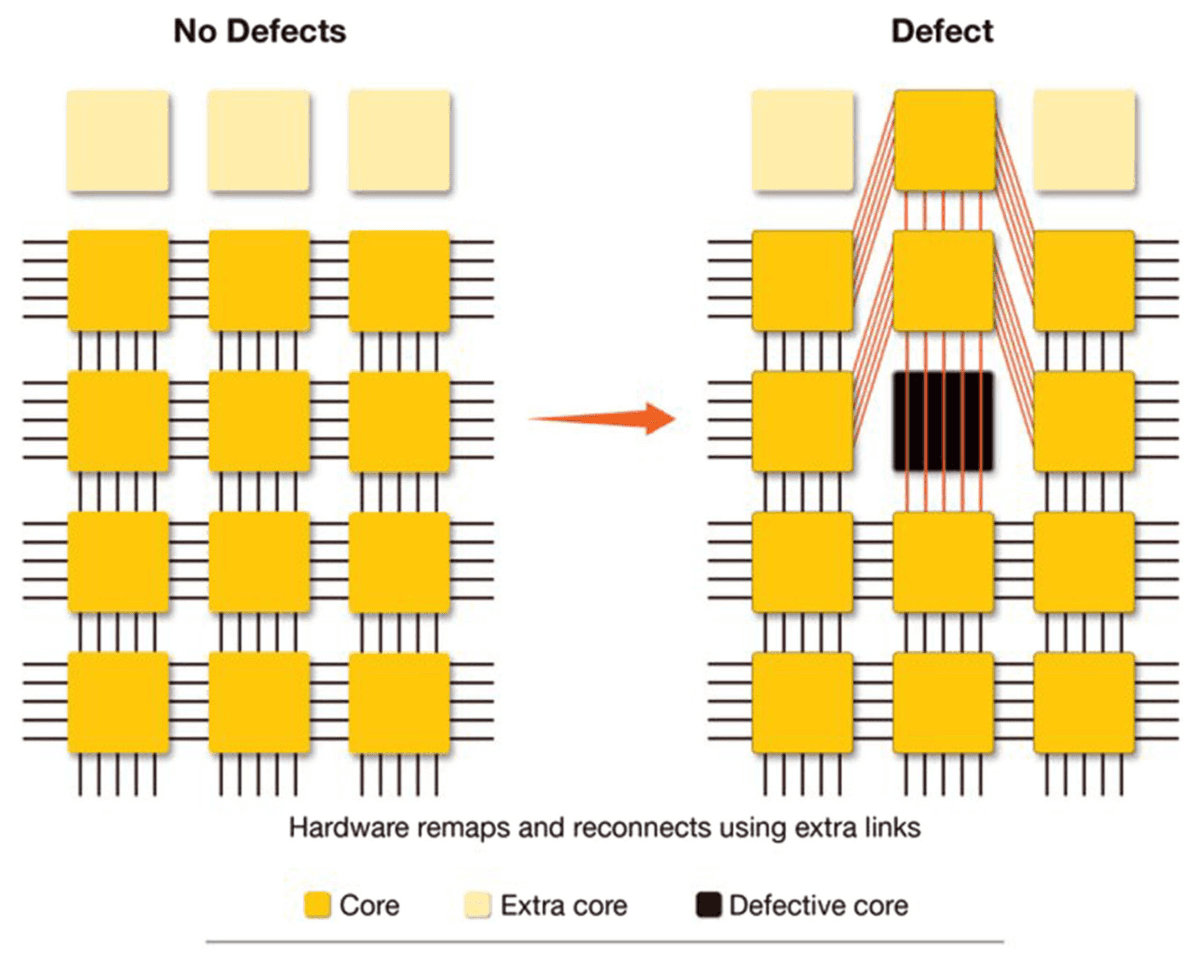
In addition, Cerebras has developed an advanced routing design that can dynamically reconfigure the connections between cores, so that when a defect occurs, the system automatically uses redundant communication paths to work around the defect.
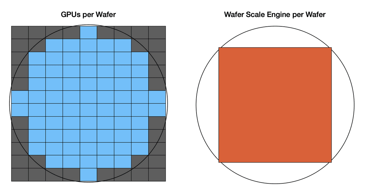
The actual manufacturing process of a conventional GPU and the WSE chip developed by Cerebras can be compared as follows. The circle represents a silicon wafer, the left is a conventional GPU, and the right is a WSE. Conventional GPUs manufacture multiple chips on a single wafer, but WSEs are manufactured as a single giant chip.
At the time of writing, TSMC's manufacturing process for the 5nm node
has a defect rate of about 0.001 per square millimeter . If defects occur at this rate, a conventional GPU would have to invalidate 361 square millimeters of space, but because the WSE-3's core size is smaller, it only has to invalidate 2.2 square millimeters of space.
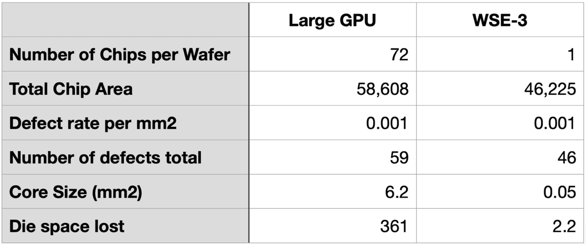
In this way, Cerebras succeeded in manufacturing a chip with a huge area about 50 times that of a conventional GPU while achieving a high silicon utilization rate of 93%.
In fact, Cerebras' AI inference service can infer data 22 times faster than when using the NVIDIA H100, and the cost is about one-fifth, which is an astounding figure.
Cerebras announces explosive AI inference service 22 times faster than NVIDIA H100, demo page also released so I tried it out - GIGAZINE

Related Posts:
in Hardware, , Posted by log1d_ts
