What is the content of the 'FPGA' that can change the circuit structure adopted by Microsoft and Amazon?

'
Reverse-engineering the first FPGA chip, the XC2064
http://www.righto.com/2020/09/reverse-engineering-first-fpga-chip.html
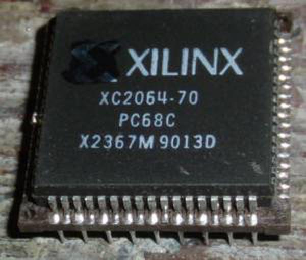
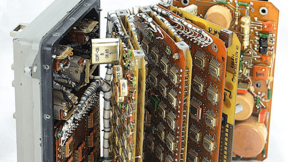
The first FPGA 'XC2064' developed by Xilinx in 1985 was said to have a much simpler structure than modern FPGAs. Nowadays , FPGAs can be programmed in standardized languages such as Verilog, but at that time Xilinx's 'XACT' required expensive software that cost as much as $ 12,000.
The basic structure of the FPGA is shown in the figure below. The blue logic block called ' CLB (Configurable Logic Block)' is interconnected with other CLBs and I / O that inputs and outputs signals.
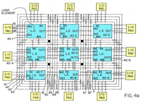
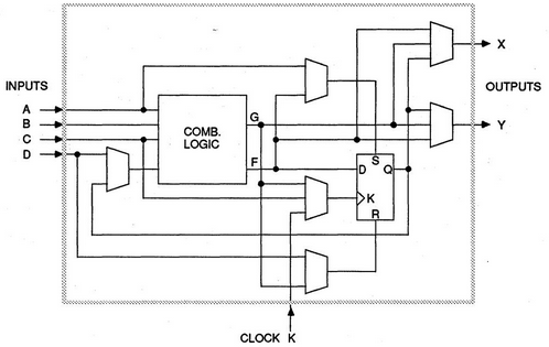
CLB is a circuit that outputs two outputs for four inputs, and is the part that makes it possible to change the circuit structure. It is equipped with a combinational circuit that can program an arbitrary circuit and a flip-flop circuit that can hold 1-bit information, and this structure is called a ' LUT (Lookup Table)'.
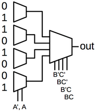
The structure of the combinational circuit in XC2064 is like this, and the multiplexer makes it possible to program the combinational circuit by selecting the data in the memory according to the input. The data is selected according to the control input represented by 'A', 'B', and 'C'.
The XC2064 is equipped with 64 CLBs, and it is the green 'switch matrix' that enables complex interconnection between CLBs. Communication between CLBs is done via this switch matrix.
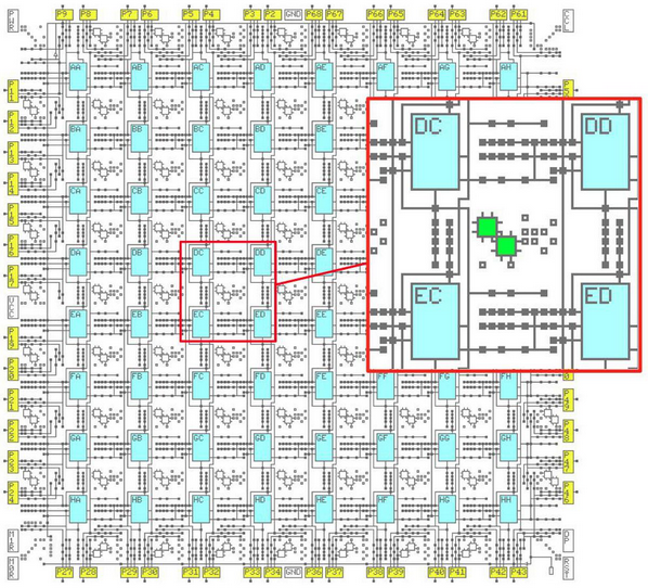
The above is the structure of FPGA, but the implementation by XC2064 is a little different. The XC2064 has 64 'tiles' that combine CLB and route control functions, and the tiles are connected to each other. Not all tiles are in close contact, with two 'buffers' for signal amplification, one in the horizontal and one in the vertical, represented by the green line in the image below. The orange line is the power, and the red 'Shift register' and the blue 'Column select' are important structures for the XC2064 to save programming settings.
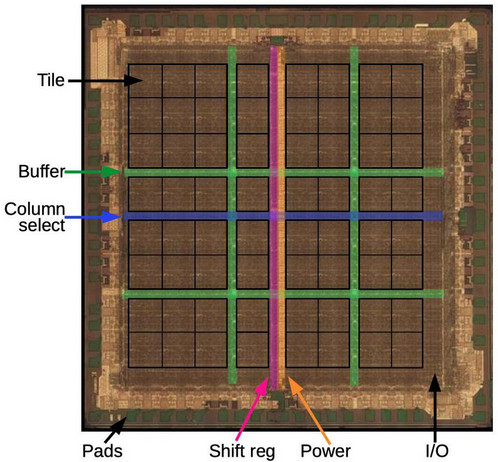
This is an enlarged image of the tile. The area surrounded by the green frame is the area for storing the programmed settings and occupies 40% of the entire tile. CLB parts such as flip-flop circuits and LUTs and route control parts such as switch matrices are mounted on other parts.

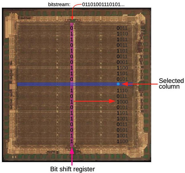
Here's how the XC2064 reads the programming settings. The memory of XC2064 can hold 160 bits in the horizontal direction and 71 bits in the vertical direction, and the circuit structure set by the programming software is input to the shift register as a 'bit stream'. After the shift register is filled with 71-bit bit strings, the column selector selects 'Which column of memory to load the current shift register value into'. In this way, the next bitstream is read into the shift register, and the column shift moves column by column, so that the bitstream is loaded into all memory.
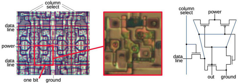
When you expand the memory circuit that saves 1-bit settings, it looks like this. The circuit diagram clearly shows the structure of reading data from the data line activated by column select.
The XC2064 uses a variety of highly optimized circuits, but initially it was difficult to manufacture and costly. Although the XC2064 sold less than modern FPGAs, it was the catalyst for a revolutionary new product, Shirriff said.
Related Posts:


in Hardware, Posted by darkhorse_log