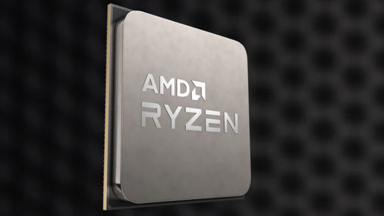
WikiChip explains AMD's next-generation architecture 'Zen 2' adopted by 3rd generation Ryzen

We will commercialize a CPU that adopts 3rd generation "Zen" microarchitecture " Zen 2 " AMD manufactures in 7 nm process in 2019. WikiChip Fuse, an information site for semiconductor technology, describes AMD's product roadmap including the CPU code name " Rome " already announced at EPYC for servers.
AMD Discloses Initial Zen 2 Details - WikiChip Fuse
https://fuse.wikichip.org/news/1815/amd-discloses-initial-zen-2-details/
◆ Zen 2 microarchitecture
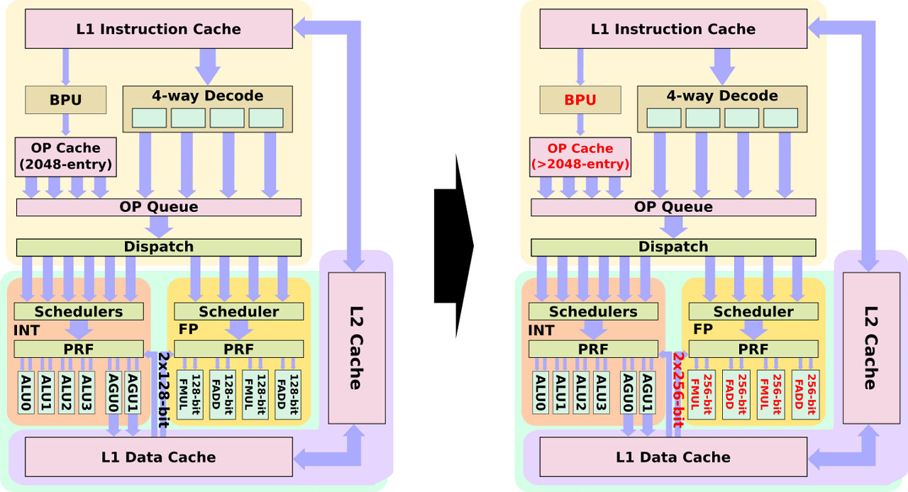
The third generation Zen microarchitecture "Zen 2" following Zen, Zen +, CPU cores are manufactured by TSMC's 7 nm process. Extended functions are greatly enhanced in the Zen 2 generation, and in order to improve throughput, the front end is adjusted and the branch prediction unit is reconstructed. This includes many improvements of prefetching and unpublished optimization for the instruction cache.
Floating point unit has been changed in back end improvement. Among them, the expansion of the data bus is impressive, AVX instruction realized by two 128-bit micro OP so far can be executed with one 256 bit wide data path. In addition, increasing both dispatch bandwidth and retire bandwidth increases IPC (number of instructions executed per clock), and mitigation measures of vulnerability Specter, which was introduced by Zen / Zen + firmware update, It has been introduced.
As a result of investigating both the 10 nm process and the 7 nm process, AMD said that it has given a go-ahead to the 7 nm process that can realize high density with lower power consumption. AMD says that by adopting the 7 nm process, the density of semiconductors will be doubled, and if it is the same power it will be 25% more performance appealing. In Computex Taipei 2018 held in June 2018, AMD claimed to boost the performance by 35%, so although it is slightly tone-down, due to the substantial improvement in performance, the third generation Ryzen has only multi-core performance It is trying to catch up with the Intel CPU and overtake even single-core performance.
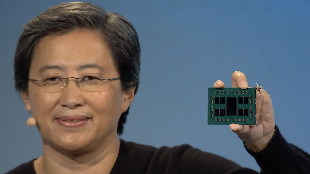
AMD has already sampled Zen 2 based chips and will be on the market in 2019.

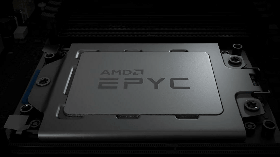
◆ Rome
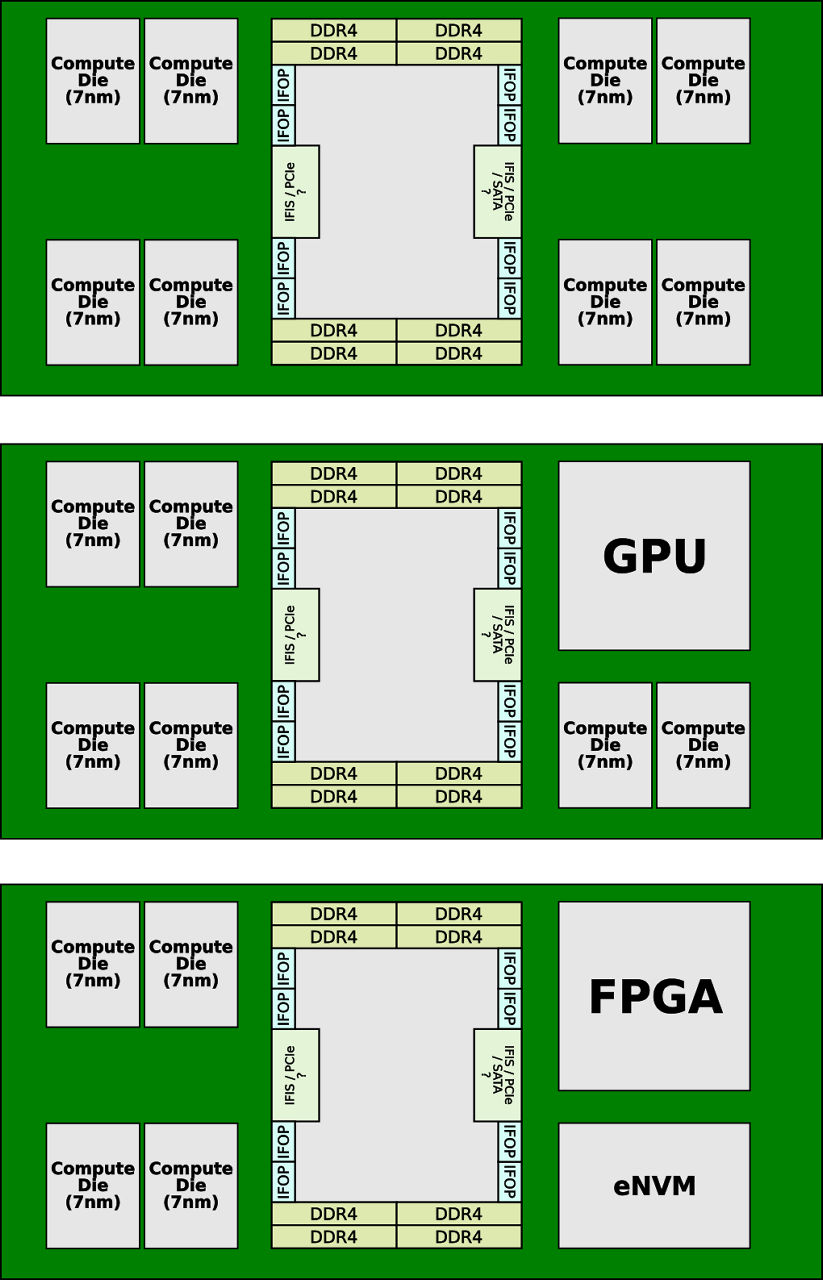
In the 2nd generation EPYC, based on the Zen 2 generation micro architecture, the code name "Rome" was adopted as a new multi-die configuration CPU.
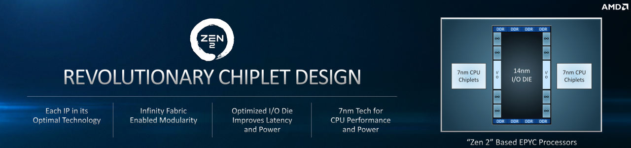
In Naple of the 1st generation EPYC, 8 CPU cores, I / O and memory interfaces were put in one die and four of these were combined to realize 32 cores, but in Rome I / O and memory The integrated I / O die that manages the center is placed in the center, and the calculation core (chiplet) is arranged around the integrated I / O die.
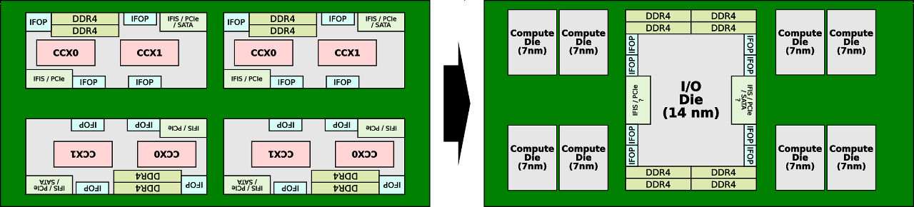
The central I / O die is manufactured in a 14 nm process and the eight chiplets (CPU die) that surround it are manufactured in a 7 nm process. Rome realizes 64 cores with 8 core dies with 8 cores. Second generation EPYC, which is 64 cores / 128 threads, doubles the throughput from first generation EPYC and increases by 4 times with AVX 2 performance.
Even in Rome PCI-Express will maintain 128 lanes, but will support a new PCI-Express Gen 4, the transfer rate will double from 8 GT / s to 16 GT / s. It also supports up to 4TB of DDR4 memory per socket with 8 channels. Assuming that the second-generation Infinity Fabric uses 16 bears as in the first generation, it will operate at 25 GT / s and the data rate is equivalent to NVIDIA's NVLink. However, AMD's Infinity Fabric can provide twice the bandwidth per link as compared to NVLink.

◆ I / O Die: WikiChip Fuse also points out the possibilities that the design of I / O dies cut out separately in the center can bring. By transferring redundant components such as I / O and south bridge to the I / O die and becoming a centralized control by the I / O die, it is possible to reduce the CPU die for calculation to other logic such as GPU or FPGA WikiChip Fuse thinks that it will be able to be replaced. " AMD has not announced such a plan, but Rome has a possibility of building a more flexible system.
◆ Road Map
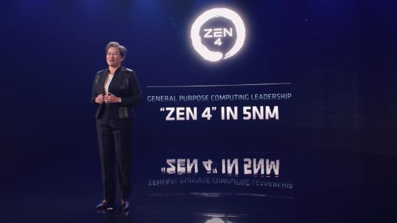
AMD also refers to the roadmap for the future. Zen 2 is scheduled to be released in 2019 as mentioned above, Zen 3 manufactured at 7 nm + thereafter is also under development as planned, further designing is going to be completed for Zen 4 further . It seems to be expected to improve the performance of Ryzen & EPYC after 2019.

Related Posts:

in Hardware, Posted by darkhorse_log