We estimate the structure of Google's machine learning machine "2nd Generation TPU" from published pictures
Google announced the second generation "TensorFlow Processing Unit (TPU)" optimized for machine learning at Google I / O 2017 held the other day. However, since Google does not clarify the detailed specification of the 2nd Generation TPU (TPU 2), I do not know the structure of TPU 2. So, Paul Teich, a chief analyst at TIRIAS Research for cloud computing and data analysis, speculates specs from published pictures.
Under The Hood Of Google's TPU 2 Machine Learning Clusters
https://www.nextplatform.com/2017/05/22/hood-googles-tpu2-machine-learning-clusters/
The first generation TPU (TPU 1) was 23 TOPS with 16 bit operation (FP 16), whereas the TPU 2 has 45 TFLOPS capability by floating point calculation. TPU 1 was an accelerator to connect to the motherboard with a PCI - Express (x8) connector. TPU 1 has no schedule function and virtualization is also impossible. It connects to the processor board and acts as a simple matrix coprocessor. Incidentally, Google does not clarify how many TPU 1 can be inserted and used on one motherboard.
On the other hand, the TPU 2 board announced at Google I / O 2017. In addition, Google utilizes TPU 2 as an in-house machine, and boards and servers equipped with TPU 2 will not be sold externally. Users can borrow machine power of TPU 2 through the TensorFlow Research Cloud (TRC) program.
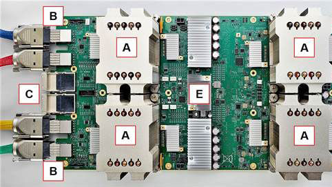
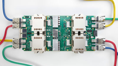
The first thing that Teich noticed when looking at the pictures of Google's public pods is that "TPU 2 is connected to one processor board with two cables." "Although it is not unlikely that TPU 2 will be connected to two different processor boards, TPU 2 and the processor board will be connected 1: 1 in order not to complicate installation tasks, programming, and scheduling." I believe.
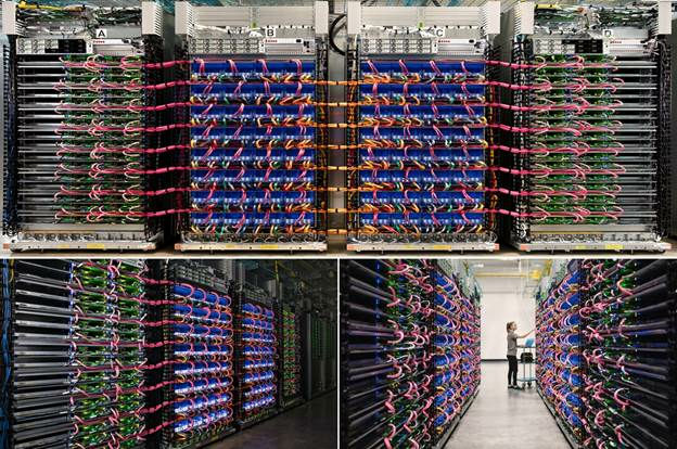
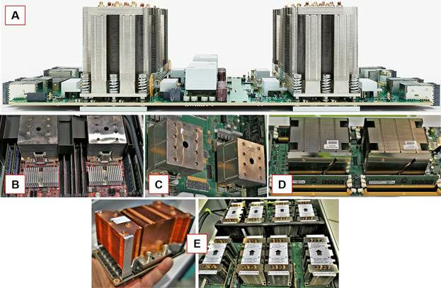
Image of TPU 2 stamp. A is "CPU rack", B and C are "TPU 2 rack", D is "CPU rack", and the blue part is a solid box. The system is designed with stamps that fit in 4 racks, and it consists of one "pod" in 4 rack units. The four stamps contain 1024 TPU 2 chips.
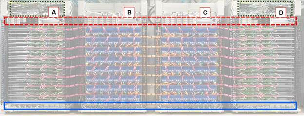
Google has released three different pictures on the TPU 2 stamp, but all the configuration and wiring of the rack looks the same. Cable color coding makes comparison easier.
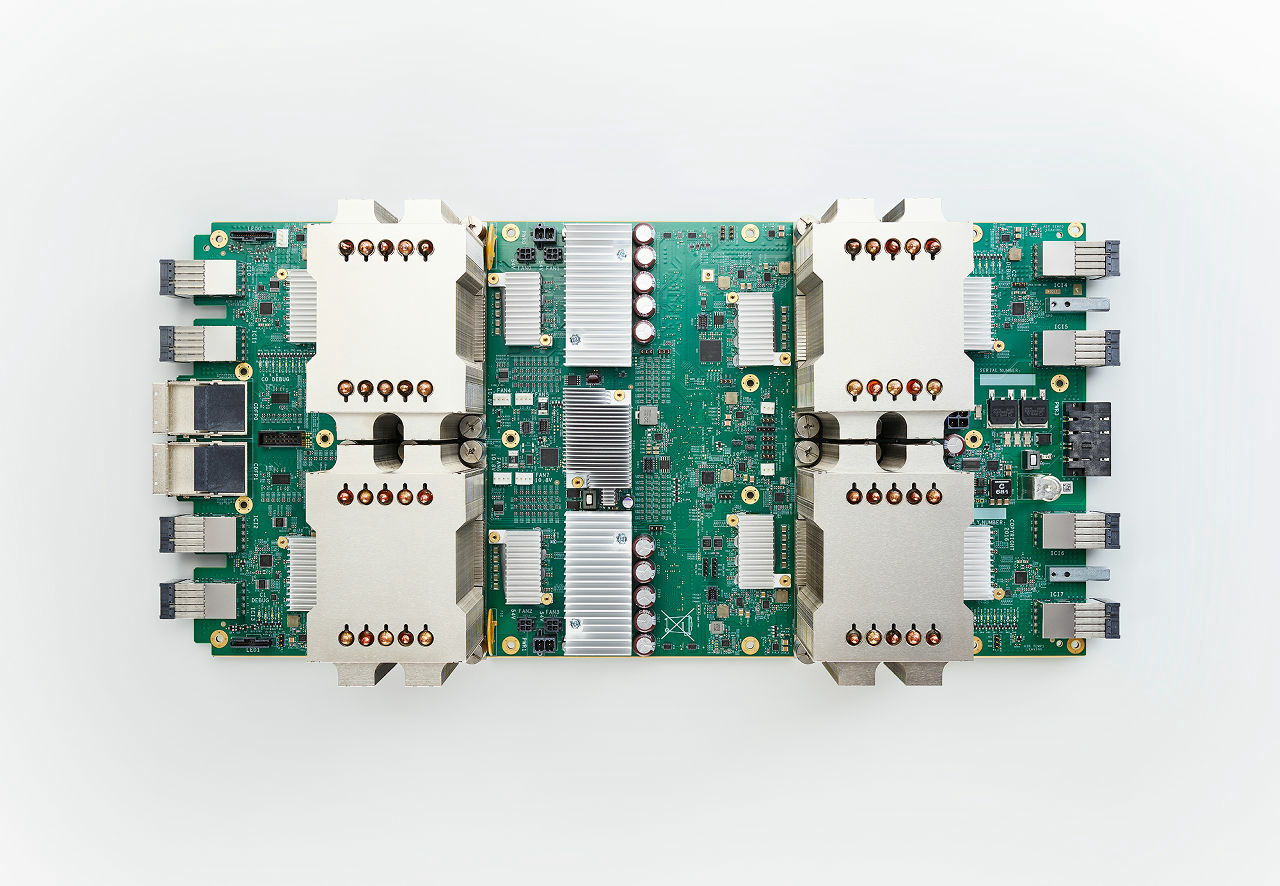
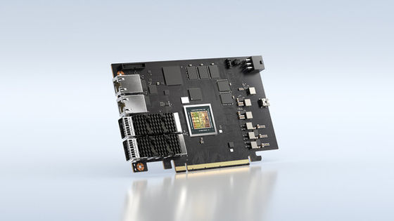
On one board, four TPU chips are mounted under the heat sink (A). BlueLink (25 GB / s) cable (B) extending two per TPU 2, Omni-Path Architecture (OPA) cable connector (C) per board, power connector (D), network switch (E) Mr Teich guesses whether it is a composition or not.
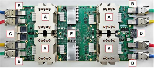
Four connectors in the shape of a square that I have not seen on the front panel. Since Google is a member of OpenCAPI and is a founding member of the OpenPower Foundation, it makes sense to think of these as BlueLink. By the way, at IBM's BlueLink, it seems that 25 GB / s per sub link is outputted in 8 directions and a signal lane of 200 GB / s (total of 16 lanes) is defined. Since there are color-coded stickers under the copper cable of BlueLink or OPA, Teich points out that there is a plan to develop a TPU 2 stamp on a large scale using color codes.

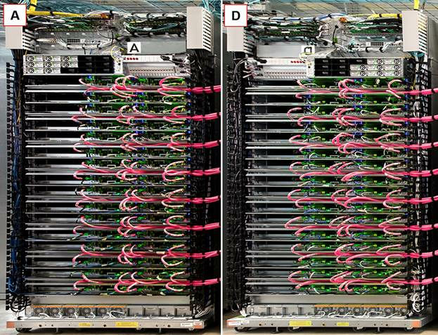
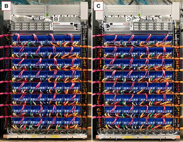
The rack configuration of the TPU 2 stamp is symmetrical. Note that the image of D in the figure below is being compared by inverting left and right so that it is symmetrical. The height of Google's rack unit is 1.5 inches smaller than industry standard 1.75 inches.
Likewise, C is an inverted image. "Although we can not accurately determine the network topology from Google's published images, it looks like some sort of hyper mesh network is built," says Teich.
The CPU board that matches the form factor of 1.5 inch server unit is Intel Xeon dual socket compatible motherboard. However, AMDEPYCBecause Qualcomm's Centriq compatible server equipped with compatible server and ARM chip is single socket specification, it seems that there is a possibility that the configuration of dual socket motherboard used by TPU 2 may change in the future.
Also, Mr. Teich guesses that if one TPU 2 board is connected to each CPU board, it will reach the total bandwidth of 25 GB / s via the OPA cable. In a general deep learning machine, the connection ratio between the GPU accelerator and the CPU is 4: 1 to 6: 1, whereas the TPU 2: Xeon CPU has a characteristic value as low as 2: 1 is. This may be because TPU 1 inherited the thought that was more friendly to FPU (floating point unit) than GPU.
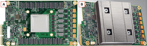
A TPU 2 board (A) with an overwhelmingly large heat sink compared to other server boards from B to E. It is almost 3 inches (about 7.6 centimeters) for two rack widths, and the size of the heat sink tells us that the power consumption exceeds 200 W respectively.
Teich also considers the power consumption of the TPU 2 system. According to Google, 1000 TRUs (exactly 1024 TPU 2 chips) are used. From there, it is estimated that the power consumption of the TRC computing with full power is 0.5 megawatts (500,000 W). The initial cost of a TPU 2 unit consisting of four stamps is one at the time of introduction, and although it is not a big deal, Teich says that running costs of 0.5 megawatts will be inconvenient for Google-level companies. If, in the future, Google will use TPU 1 for a year, it may be a testament to the fact that Google is seriously considering the power cost of TPU 2.
Related Posts:

in Hardware, Posted by darkhorse_log