Successfully manufactured '3D chip' that is expected to significantly improve performance compared to existing 2D semiconductors
Instead of semiconductors with parts laid out on a flat surface, they developed a '3D chip' in which layers of parts are stacked vertically. This has resulted in significant improvements, such as a four-fold increase in throughput compared to conventional '2D chips.'
Researchers unveil groundbreaking 3D chip to accelerate AI | Stanford Report
First truly 3D chip fabbed at US foundry, features carbon nanotube transistors and RAM on a single die — future devices could have up to 1000x improvement in energy-delay product | Tom's Hardware
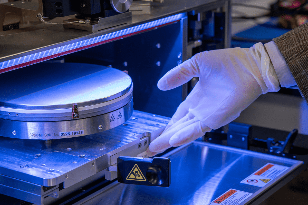
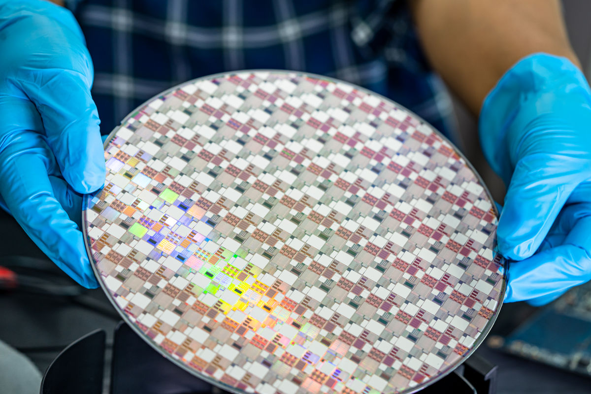
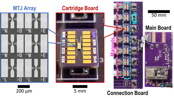
The research and development, conducted by engineers from Stanford University, Carnegie Mellon University, the University of Pennsylvania and the Massachusetts Institute of Technology in collaboration with semiconductor foundry company Skywater Technology, resulted in the first 3D chips developed in a commercial foundry.
Modern AI models like ChatGPT and Claude must shuttle massive amounts of data between the memory where the information is stored and the computing units where it is processed.
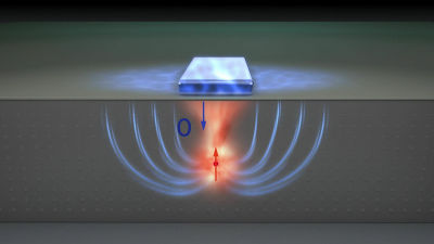
In traditional 2D chips, components are arranged on a single plane and memory is distributed over a limited area, forcing data to travel along several long, congested paths. The inability to place enough memory close together on the chip creates a bottleneck, forcing the system to constantly wait for information. Engineers call this the 'memory wall' and view it as a limitation of existing chip designs.
For decades, chipmakers have tried to address the memory wall by shrinking the tiny switches called 'transistors' that perform calculations and store data, and packing more of them onto each chip. But this strategy was approaching a physical limit that researchers call the 'miniaturization wall.'
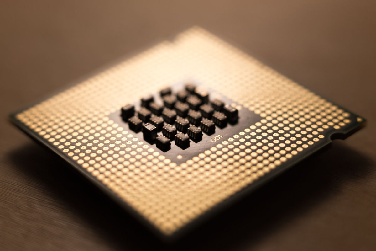
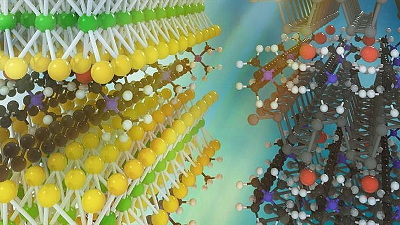
New 3D chips are semiconductors that improve performance by vertically integrating memory and computing. While '3D chips' have existed in the past, most have relied on stacking individual chips, which left the connections between layers loose and prone to bottlenecks. Instead of manufacturing separate chips and then fusing them together, Stanford researchers have built the layers in a 'monolithic' way, stacking each layer in a continuous process. This allows for much denser connections between components.
'3D chips can move much more information at high speeds, much like elevators in a high-rise building move many occupants at the same time,' said Tathagata Slimani, lead author of the paper and assistant professor of electrical and computer engineering at Carnegie Mellon University.
In early hardware tests, the 3D chip prototype demonstrated approximately four times the performance of a comparable 2D chip, and simulations of a higher-layer version with more memory and compute units showed even greater performance gains. The higher-layer version demonstrated up to 12 times the performance improvement in real-world use cases, including Meta's AI 'LLaMA' model.
While experimental 3D chips have been developed in the past, this is the first time they have demonstrated clear performance improvements and been manufactured in a commercial foundry.
Most notably, the researchers say their design paves the way for a 100x to 1000x improvement in the energy-delay product (EDP), a key metric for balancing speed and energy efficiency. By dramatically shortening data movement and adding more paths, the chip promises to achieve both high throughput and low power consumption per operation, something previously considered unattainable with conventional planar architectures.
'This research shows that these advanced architectures can be produced not just in the lab, but at scale domestically,' said Mark Nelson, co-author of the paper and vice president of Technology Development Operations at SkyWater Technology. 'This is exactly what America needs to be at the forefront of semiconductor innovation.'
Related Posts:


in Hardware, Posted by log1p_kr