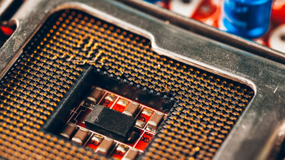
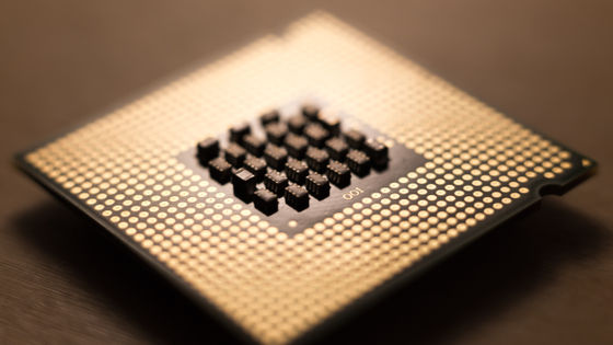
A "super" superlattice is created that leads to realization of a computer capable of extremely high speed operation
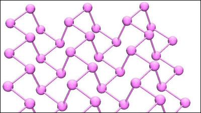
A plurality of extremely thin crystal lattices where the thickness is only one atom to several atoms are superimposed "Super lattice"Is expected to lead to the realization of the next generation of electronic chips, and ultimately, computers capable of ultra high speed operation. And this time, the result of the research which advanced the technology further step was brought by the research team of UCLA (University of California Los Angeles).
Super 'superlattices' could enable 'superfast' transistors
http://www.newelectronics.co.uk/electronics-news/super-superlattices-could-enable-superfast-transistors/170605/
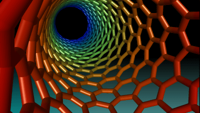
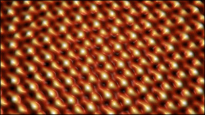
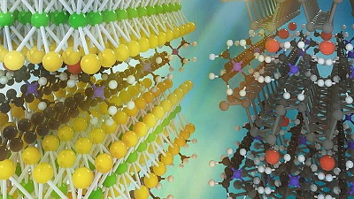
Since the superlattice has only atomic level thickness as mentioned above, it is also called "2D material" (2D Materials) which is a virtual plane (2D). In previous technologies, we could only realize stacking layers with similar atomic structure, whereas the research team made it possible to stack layers having different structures and totally different electric characteristics and functions It is.
In the "super" superlattice developed by the research team, it is possible to build an electrically insulating layer by stacking insulators on a certain conductor layer, and to construct a highly compact and highly efficient semiconductor about. In addition, its manufacturing process is said to be faster and more efficient than conventional technologies. There is a possibility that layers can be made up to thousands of superlattices, which means that only this new technology can realize this.
Professor Yu Huang said, "Traditional semiconductor superlattices could only be realized with elements with extremely high lattice symmetry.We have completely different layers, each layer is perfect We realized for the first time a stable superlattice structure with atomic structure.The superlattice structure of this time can have different electrical characteristics depending on the application and it is used for potential technical use and further scientific research It is possible. "
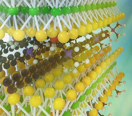
In order to realize this new structure, the research team enters another molecule between the moleculesIntercalationThe application of the electrochemical intercalation method which electrochemically causes the chemical reaction called is applied. First of all, using black phosphorus (black · phosphorus) to make the underlying 2D layer, we succeeded in composing the layer by putting ammonia molecules having multiple size and structure there. It seems that it is possible to change the electrical characteristics of each layer according to demand.
This result also leads to the development of the next generation semiconductor device. Professor Xiangfeng Duan of the research team says, "With this result it will be possible to make transistors that are faster but less power consuming and more efficient light emitting devices."
Related Posts: