A fierce warrior who succeeded in 'GPU development from scratch' in just two weeks with no experience
I've spent the past ~2 weeks building a GPU from scratch with no prior experience. It was way harder than I expected.
— adammaj (@MajmudarAdam) April 25, 2024
Progress tracker in thread (coolest stuff at the end)👇 pic.twitter.com/VDJHnaIheb
Step 1: Learn the basics of GPU architecture
Adammaj first tried to understand how modern GPUs work at an architectural level, which turned out to be a much more difficult task than he expected, as GPUs are a highly proprietary technology and there are no online learning resources to learn more about GPU architectures.
Adammaj started by learning NVIDIA's CUDA and trying to understand the patterns of GPU software, which allowed him to understand the SIMD programming patterns used to create GPU programs, called kernels.
From there, Adammaj decided to study the core elements of GPUs in detail. The outline of the core elements of GPUs he learned is as follows:
Global Memory: External memory for storing data and the programs that access it is a major bottleneck and constraint in GPU programming.
Computing core: The main computing unit that executes kernel code in parallel in different threads.
Hierarchical cache: A cache that minimizes access to global memory.
Memory Controller: For handling throttling requests to global memory.
Dispatcher: The main control unit of the GPU that distributes threads among available resources for execution.
In addition, the main units in each computing core are also studied, and the outline of the main units learned by adammaj is as follows:
Register: A dedicated space for storing data for each thread.
Local/Shared Memory: Memory that is shared to pass data between threads.
Load Store Unit (LSU): A unit used to store/load data from global memory.
Computing unit: A general term for ALUs, SFUs, dedicated graphics hardware, etc. that perform calculations on register values.
Scheduler: The unit that manages the resources of each core and plans when instructions from different threads are executed. This is where much of the complexity of GPUs resides.
Fetcher: A unit that retrieves instructions from program memory.
Decoder: A unit for decoding instructions into control signals.

As he learned the basics of GPU architecture, Adammaj wrote, 'GPUs are so complex that I realized that if I didn't limit myself to only what I needed for my design, my project would become extremely bloated.'
Step 2: Build your own GPU architecture
Adammaj started building his own GPU architecture based on what he learned. Adammaj's goal was to 'create a minimalist GPU that would highlight the core concepts of GPUs, eliminate unnecessary complexity, and make it easier for others to learn about GPUs,' so designing his own architecture was 'a great exercise in determining what is really important.'
Adammaj said that he decided to emphasize three points in building the GPU architecture: 'We wanted to highlight the broad use cases of GPUs for general-purpose parallel computing (GPGPU) and machine learning (ML), so we decided to focus on core capabilities rather than graphics-specific hardware.'
Parallelism: How are SIMD patterns implemented in hardware?
Memory Access: How do GPUs address the challenge of accessing large amounts of data from slow, bandwidth-limited memory?
Resource Management: How does the GPU maximize resource utilization and efficiency?
The GPU architecture that adammaj built himself is shown below. He explained, 'After repeated iterations, we finally arrived at the architecture that we implemented in the actual GPU.' In addition, the GPU architecture is represented in its simplest form in the diagram below.

Step 3: Create custom assembly language for the GPU
The most important question is whether the GPU can actually execute kernels written in the SIMD programming pattern. To make this possible, it seems necessary to design a unique
To achieve this, Adammaj took inspiration from LC4, an ISA, to create his own ISA, and even wrote some simple matrix calculation kernels as a proof of concept.
Below is a table summarizing the exact structure and encoding contents of the ISA that adammaj designed.

◆ Step 4: Write a matrix calculation kernel using ISA
Now that we have our own ISA, we create two matrix calculation kernels to run on the GPU. Each kernel specifies the matrix to operate on, the number of threads to launch, the code to run on each thread, etc.
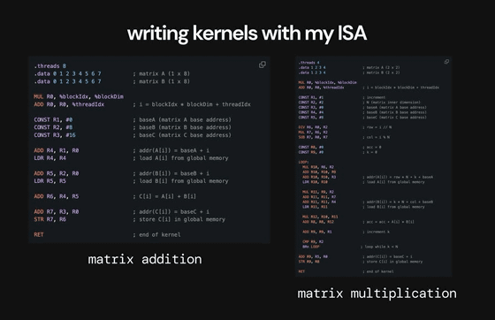
Adammaj's matrix addition kernel uses eight threads to add two 1x8 matrices and demonstrates the use of SIMD patterns, some basic arithmetic instructions, and load/store functions. He also created a matrix multiplication kernel, which uses three threads to multiply two 2x2 matrices and is designed to demonstrate branching and looping.
'Given the most recent use cases for GPUs in both graphics and machine learning, they revolve around matrix computations (with much more complex kernels), so demonstrating the matrix computation capabilities was important,' said Adammaj.
The matrix addition kernel and matrix multiplication kernel created by adammaj are as follows.
Step 5: Build the GPU in Verilog and run the kernel
They then started designing the GPU in Verilog , which adammaj says was 'by far the most difficult part, as we ran into a lot of issues and had to rewrite the code multiple times.'
Through multiple code rewrites, adammaj wrote, 'When I encountered memory issues, I realized why managing access from the bottleneck memory is one of the biggest constraints of the GPU.' 'It wasn't working as designed because multiple LSUs were trying to access memory at the same time, and I realized that a request queue system was necessary. At this point, I was able to fundamentally understand the need for a memory controller.' 'After implementing a simple approach to the dispatcher/scheduler, I realized that performance could be optimized by more advanced scheduling and resource management strategies such as pipelining.'
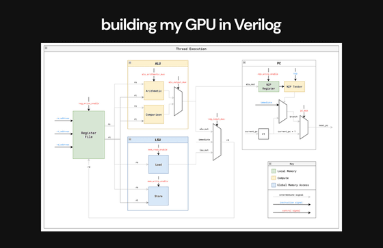
Below is the execution flow of a single thread implemented in the GPU in Verilog.
The video below shows how to run a matrix addition kernel on a GPU, look at the execution trace of the GPU as it runs, and check the end state of the data memory where the GPU saved the final result. At each cycle in the execution trace, you can see the individual instructions, PC, ALU operations, register values, etc. for each thread and core. 'The most important thing is that at the beginning, we see the empty addresses of the result matrix, and at the end, the correct values are loaded into the result matrix in data memory,' adammaj wrote.
After tons of redesigns, finally running my matrix addition & multiplication kernels and seeing things work properly and my GPU output the correct results was an incredible feeling.
pic.twitter.com/WB6PqblK31 — adammaj (@MajmudarAdam) April 25, 2024
Here's a video of me running the matrix addition kernel on my GPU, going through the execution…
Step 6: Convert the design into a full-chip layout
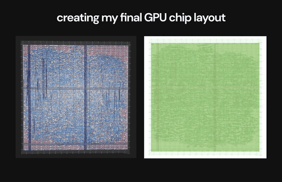
Once the Verilog design was complete, the final step was to hand the design over to an EDA flow to create the final chip layout. The process node was 130nm from Skywater and the chip was fabricated using Tiny Tapeout 6 .
While you may have a design that works in theory and in simulation, translating that design into a final chip layout using a GDS file is 'a big barrier to shipping the design,' Adammaj said. In fact, he said he ran into issues where he couldn't clear the design rules specified in OpenLane, and had to modify some of his GPU designs to solve the problem.
The GPU chip layout created by adammaj is as follows.
Details of adammaj's GPU development are also summarized on GitHub.
GitHub - adam-maj/tiny-gpu: A minimal GPU design in Verilog to learn how GPUs work from the ground up
https://github.com/adam-maj/tiny-gpu
Related Posts:
