What is 'conspicuous power-up' that Intel has given to Ice Lake generation CPUs?
The more
Ice Lake Store Elimination | Performance Matters
https://travisdowns.github.io/blog/2020/05/18/icelake-zero-opt.html
Hardware Store Elimination | Performance Matters
https://travisdowns.github.io/blog/2020/05/13/intel-zero-opt.html#hardware-survey
This time Downs paid attention to the execution speed of ' Intel AVX, ' which is one of the CPU instruction sets. Intel AVX is an instruction set installed from the Sandy Bridge generation, and there are three generations, AVX, AVX2, and AVX-512. This technology is mainly used for image processing and video encoding, and it also supports the instruction set used in neural networks.
This is the C ++ code prepared by Downs to test the performance of AVX. A code that fills memory with a specific value, val.
[code] std :: fill (buf, buf + size, val); [/ code]
The following is a partial excerpt of the assembly language output by compiling this C ++ code. The compiler uses GCC 9.2.1.
[code] .L4:
vmovdqu YMMWORD PTR [rax + 0], ymm1
vmovdqu YMMWORD PTR [rax + 32], ymm1
vmovdqu YMMWORD PTR [rax + 64], ymm1
vmovdqu YMMWORD PTR [rax + 96], ymm1
vmovdqu YMMWORD PTR [rax + 128], ymm1
vmovdqu YMMWORD PTR [rax + 160], ymm1
vmovdqu YMMWORD PTR [rax + 192], ymm1
vmovdqu YMMWORD PTR [rax + 224], ymm1
add rax, 256
cmp rax, r9
jne .L4 [/ code]
'Vmovdqu', which is an instruction to load and store in AVX2, is used, and the value of the 'ymm1' register is written to the memory in units of 32 bytes. At this time, the memory address is expressed using the value of general-purpose register 'rax'.
[code] vmovdqu YMMWORD PTR [rax + 0], ymm1 [/ code]
In this way, the process is executed while shifting the memory address by 32 bytes.
[code] vmovdqu YMMWORD PTR [rax + 0], ymm1
vmovdqu YMMWORD PTR [rax + 32], ymm1
vmovdqu YMMWORD PTR [rax + 64], ymm1 [/ code]
When the area of 256 bytes of memory can be filled with the value, 256 is added to the value of the general-purpose register to prepare for the next loop.
[code] vmovdqu YMMWORD PTR [rax + 224], ymm1
add rax, 256 [/ code]
Using the Sky Lake generation Core i7 6700HQ, execute the program above, and the graph shows the writing speed when the value to fill the memory is set to '0' and '1'. It is fast when inputting the data of the size that can fit in the L1 cache, but it can be seen that the writing speed decreases as the data size increases and overflows into the L2 cache, L3 cache, and RAM.
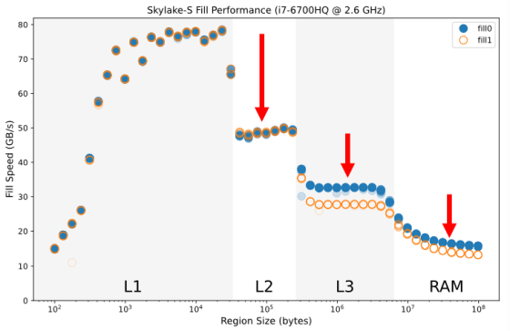
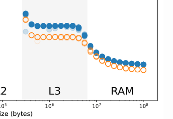
In addition, regarding the size of data that uses the L3 cache and RAM, there is a difference in speed between when 0 is written and when 1 is written. Regarding this, Downs said, `` When writing 0, the writing speed is increased because the performance optimization is performed in the operation of writing the data overflowing from the L2 cache to the L3 cache and writing the data from the L3 cache to the RAM. It goes up a little. '
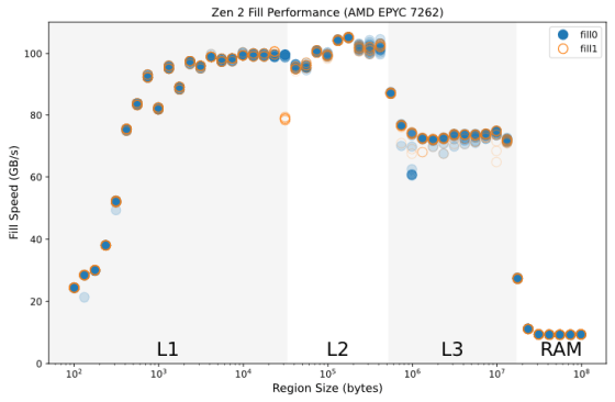
This performance optimization cannot be seen on other CPUs such as EPYC with AMD's Zen 2 architecture.
The graph below shows that the data read from the L3 cache or RAM overflows from the L2 cache and is discarded without being written to the L3 cache or RAM and is in the “Silent” state, and the data overflowing from the L2 cache overflows the L3 cache or RAM. The line graph shows the percentage of cache that is in the 'Non Silent' state that is rewritten to, and is overlaid on the previous write speed graph.
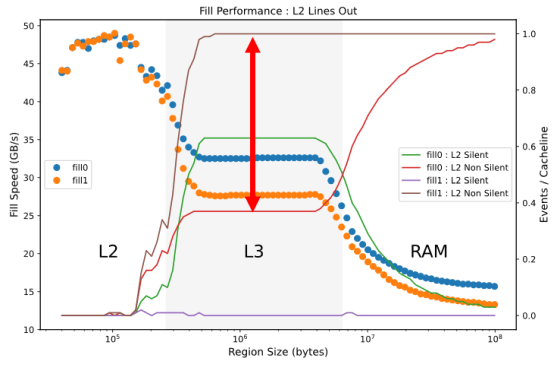
When writing data that fits in the L3 cache, when writing 0, 64% of the cache is in the green “Silent” state and 36% is in the red “Non Silent” state. When writing, the brown 'Non Silent' state cache accounts for almost 100%. In other words, when writing 1 there are many 'useless rewrites', but when writing 0, such waste is eliminated by the amount of the arrow. This is 'performance optimization' explained by Downs.
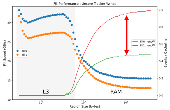
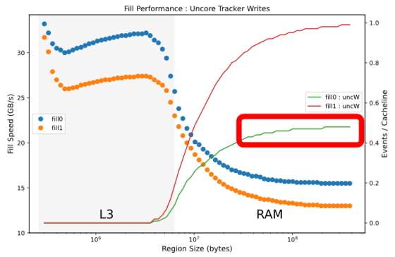
Such optimization is also done when writing data from L3 cache to RAM. When reading from the RAM to the L3 cache, the percentage of the 'UnCore' cache that writes the data overflowing from the L3 cache to the RAM again is expressed by a line graph, and it looks like this when superimposed on the writing speed. The percentage when writing with 0 is represented by the green line, and it can be seen that about half of the writing is wasted compared to the percentage when writing with 1 in red. As for the reason why such optimization is performed only at 0, Downs said, “Overwriting 0 with 0 is the most frequent operation among redundant operations, and it is also possible to determine whether the write destination is 0 or not. Isn't it easy? '
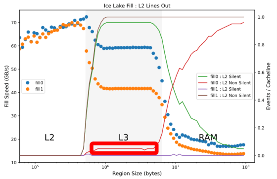
According to Downs, such CPU optimization is further advanced in Ice Lake. Looking at the benchmark results on the Ice Lake generation Core i5 1035 G4, the percentage of cache in the 'Non Silent' state when writing data from the L2 cache to the L3 cache is below 10%.
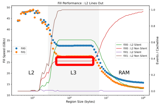
If you re-post the Sky Lake generation results, you can see that the cache in the 'Non Silent' state accounts for 36%, and the write speed by 0 is improved in the Ice Lake generation.
As for the ratio of “UnCore” cache that rewrites data from L3 cache to RAM, it can be seen that the ratio of rewrite is significantly reduced when writing 0.
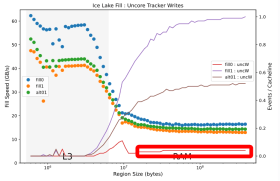
The difference is clear when compared to the graph showing the percentage of 'UnCore' cache for the Sky Lake generation.
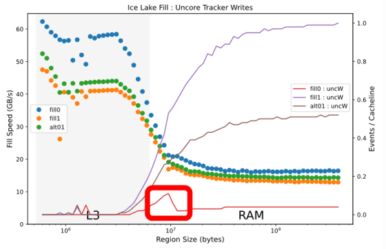
Also, there is a small peak in the number of writes by 0 near the boundary where the amount of data to be written overflows from the L3 cache to RAM, 'There may be some optimization mechanism here,' Downs commented. ..
Downs is also comparing the performance of AVX2 and AVX-512 on Ice Lake generation CPUs. If you specify '-march = icelake-client' as the architecture when compiling the program above, the AVX2 instruction set will be used.
[code] .L4:
vmovdqu32 [rax], ymm0
vmovdqu32 [rax + 32], ymm0
vmovdqu32 [rax + 64], ymm0
vmovdqu32 [rax + 96], ymm0
vmovdqu32 [rax + 128], ymm0
vmovdqu32 [rax + 160], ymm0
vmovdqu32 [rax + 192], ymm0
vmovdqu32 [rax + 224], ymm0
add rax, 256
cmp rax, r9
jne .L4 [/ code]
On the other hand, if you compile by specifying '-march = native' as the architecture, the AVX-512 instruction set using the zmm register will be used. With the AVX-512 program, 512 bytes are written in one loop.
[code] .L4:
vmovdqu32 [rax], zmm0
add rax, 512
vmovdqu32 [rax-448], zmm0
vmovdqu32 [rax-384], zmm0
vmovdqu32 [rax-320], zmm0
vmovdqu32 [rax-256], zmm0
vmovdqu32 [rax-192], zmm0
vmovdqu32 [rax-128], zmm0
vmovdqu32 [rax-64], zmm0
cmp rax, r9
jne .L4 [/ code]
Comparing the write speeds of the AVX2 and AVX-512 instruction sets for writing 0 and 1 respectively, if the data fits in the L1 cache, the AVX-512 instruction set writes 0 by 1 and 1 by 1 It is superior in both cases.
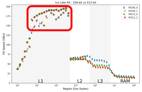
However, when writing data of a size that uses the storage device after the L2 cache, it can be seen that the writing speed by 0 of AVX2 represented by the blue semicircle is missing.
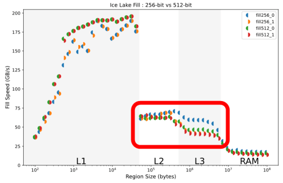
Focusing only on writes by 0 in the L2 and L3 caches, the ratio of caches in the “Silent” state is higher in AVX2 (green line), and caches are efficiently discarded and optimization is further advanced. You can see that. Downs commented, 'It's complicated and I don't understand.'
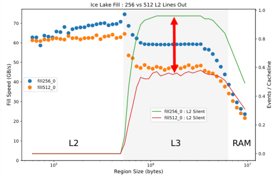
In conclusion, Downs explained that the optimization of write by 0 that was confirmed in the Sky Lake generation is still alive in the Ice Lake generation, and its performance is almost doubled. Also, in the Ice Lake generation, it is said that AVX2 is superior to AVX-512 when writing by 0 that is larger than the size of the L1 cache occurs.
Related Posts:
