If there is no Korea, the modern society will collapse "Transistor" structure explained in the movie
Small electronic components "A transistor"Hundreds of millions of people are used in smartphones and PCs, which are indispensable to many people, as well as running a train, shedding music from speakers, and skipping rockets to space, modern It is absolutely indispensable to establish a civilized society. A movie explaining how such a transistor operates in a mechanismTransistors, How do they work?"Is published on Learn Engineering on YouTube channel.
Transistors, How do they work? - YouTube
Transistor invention has brought innovative changes in people's lives.

Of course, it is also incorporated in the processor built in the smartphone and it is the point of operation.

Such a transistor has two main roles. One role is to operate as a "switch" of the electric circuit.

Another role is to "amplify a weak current" such as a microphone.

As the material of the transistorsemiconductorIs used. In the transistor introduced in the movie,Silicon (silicon)We explain the structure of the transistor using as the main raw material.

When silicon is expanded to atomic level, it looks like this.

A silicon atom has four electrons (light blue) and bonds with four adjacent silicon atoms.

In the movie, to explain in a visual and easy-to-understand manner, I will describe and describe silicon atoms as cute "smileies".

Adjacent smileys are cross-linked and strongly linked to each other by covalent bonds. The state of this covalent bond does not cause charge change by movement such as electrons. In other words, it means "insulated" state where electricity does not flow.

However, with this, it can not be used as an electronic device. Therefore, in silicon semiconductors, in order to allow electricity to flow, "dopingI will use the method called. There are two methods for doping. The first method is "N type doping"is. In this method,Rin(N-type dopant) as a material such as "a material having one valence electron compared to the valence electron of a semiconductor" to generate electricity remaining in the semiconductor to allow electricity to flow is.

Another doping method is "P type doping"is. In this method, contrary to impurities added to N-type doping,BoronSuch as "atom with one less valence electron" as a P type dopant. Then, a state where one electron enclosed by the yellow green line of the image is missing is "Hole"Occurs inside the semiconductor. P type doping is to make electricity flow by flowing electrons into this hole.

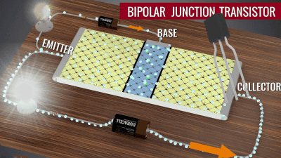
In the basic structure of the transistor, doped semiconductors are alternately stacked on three layers. The image transistor is sandwiched between an N type doped semiconductor (N type semiconductor) which is expressed in yellow from the left and a P type doped semiconductor (P type semiconductor) and N type semiconductor which is represented blue.

In the movie, I will explain using this doped three layer semiconductor. However, before explaining how the three layers work suddenly, in the movie, two layers of semiconductors with N and P,diodeIt will briefly explain how it works.

The diode consists of a P type semiconductor (blue) with insufficient electrons and an N type semiconductor (yellow) with electrons remaining.

Inside the diode, "P-type semiconductor" and "N-type semiconductor" are in a "short" or "left" relationship with each other in electrons, and electrons are delivered in the boundary happen. When delivery takes place at the boundary, the P-type semiconductor (blue) receives electrons and is slightly "negatively" charged. On the other hand, the N type semiconductor (yellow) emits electrons, so it charges slightly "positively". Then, "boundary line part (red)" is a perfectly suited region without electrons "Depletion layer(Depletion Layer) is born. The depletion layer becomes a region where there is no "carrier" that carries the charge, so here "electric insulation layer" is born.

Connecting a power supply to this diode, applying a voltage to the N side plus the P side and a negative voltage to the P side spreads the "depletion layer" area where electricity does not flow. This state is called "reverse bias".

Next, turn over the power supply and consider the case where the direction of the current reverses.


When the power supply is set in the opposite direction, the electrons remaining in the N type semiconductor toward the P type semiconductor where electrons are depleted will flow and electricity will flow. This state is called "forward biasing".

It is like this when showing the whole circuit in the forward bias state. Electrons are attracted to the positive pole of the battery and flow through the circuit to the negative pole, so that electrons flow in the image circuit counterclockwise. In this way, it is the diode that can flow electricity only in one direction.

Next, we will make the transistor into three layers of semiconductors, and we will move on to the explanation of "circuit incorporating transistor". The middle P-type semiconductor (blue) seems to be thick for explanation, but it is made very thin with real transistors. Looking back at the circuit of the diode, looking at the circuit of the diode, it is said that it is a circuit that combines the two types of diodes "reverse bias diode circuit" and "forward bias diode circuit" in the middle I understand this. In other words, no matter what direction it is, the combination of N type semiconductor (yellow) → P type semiconductor (blue) will become the same circuit as the reverse bias diode, so electricity will not flow.

Let's extend the lead from the P type semiconductor (blue) part in the middle of the transistor and try to add a circuit with additional power supply.

If you add a power supply to the part surrounded by a red line, you can see that the transistor circuit including the power supply is the same as the "diode circuit in the forward bias state". In other words, in this part, electrons flow from the N type semiconductor to the P type semiconductor and a current is generated from plus to minus.

At this time, the phenomenon that electrons corresponding to the part of the left N type semiconductor also moves to the N type semiconductor on the opposite side through the P type semiconductor appears. In the following image, the current of the power source written as "1st POWER SOURCE" was interrupted by the N type semiconductor at the beginning, but as the first current is generated as described above, there is no obstruction Larger current will occur.

The magnitudes of the currents flowing through the two power supplies "1st POWER SOURCE" and "2nd POWER SOURCE" are very different as shown in the following figure. this is"By giving a small current first, you can create a larger currentThat means that.

The three terminals to which the power supply is connected are "BASE (base) "EMITTER (Emitter) "COLLECTOR (collector) "Is named. To describe the contents so far using this term, "When current is generated in the base, it becomes possible to transfer electrons from the emitter to the collector (= current is generated)". At this time, the current generated at the collector and the emitter is larger than the current generated at the base and the emitter. To put it simply, it means "you can make a larger current between the emitter and the collector by giving a small current to the base". This is one of the roles that the transistor has "amplification"It is expressed in the brightness of the light bulb shown in the figure below.

So far we will replace "a transistor sandwiching semiconductors in yellow, blue and yellow" with what looks like "transistor actually used". Up to this point, "a transistor sandwiching a semiconductor expressed in yellow, blue, yellow,Bipolar transistor(BJT) is what is called a kind.

It is like this when placing actual transistor elements.

If you add an additional transistor, you can further amplify the current. The direction of current flow is indicated by an orange arrow, and the amount of current is indicated by the thickness of the arrow. The circuit of the image is constructed so that the current flowing from the battery on the upper left and the current from the battery on the lower right are amplified by the transistor and merged.

When electric bulbs are installed in each place where electricity is flowed and amplified, it looks like this. From the brightness of the light bulb passed through the first transistor, you can see that the light bulb that passed through the second transistor is brighter.

By replacing the dark bulb with the microphone at the position of the dark bulb and the loudspeaker at the position of the light bulb, the current of the signal is amplified by the transistor, so the signal picked up by the microphone is connected directly to the speaker You can amplify.

In addition to signal amplification, the transistor also functions as a switch. A transistor has the characteristic that "electricity is not flowed unless a sufficient voltage is applied to the base", and it is possible to make a "switch" that controls on / off of the current.

When a sufficient voltage is applied to the base, the transistor functions as a "on" switch ... ...

On the contrary, when no voltage is applied, the circuit is shut off to create the "OFF" state. With this mechanism, it becomes possible to create "0 and 1" states, which is the basic structure of digital circuits and digital memories. By using two bipolar transistors, basic logic circuit that forms digital memory "flip flopYou will be able to configure it.

Related Posts:
