What is the mysterious holographic chip "HPU" developed by Microsoft for HoloLens?

ByMicrosoft SwedenMicrosoft Sweden
"Microsoft is under development"HoloLens"Is a goggle type device, and if you put it on it will carry the function that you had never had before to project a 3D hologram in the real world. Microsoft independently developed a chip called "HPU (holographic processing unit)" to project holograms into the real world, and the details were held in CaliforniaHot ChipsPublished at.
Microsoft's HoloLens secret sauce: A 28 nm customized 24-core DSP engine built by TSMC • The Register
http://www.theregister.co.uk/2016/08/22/microsoft_hololens_hpu/
The HPU of Microsoft's holographic dedicated chip installed in HoloLens is a 28 nm thick TSMC assembledCoprocessorWith 24 Tensilica DSP cores. HPU has 65 million logic circuits, 8 MB ofSRAM(Static RAM) · DDR3 memory installed. By adopting this HPU, calculation of 1 trillion level per second is possible.
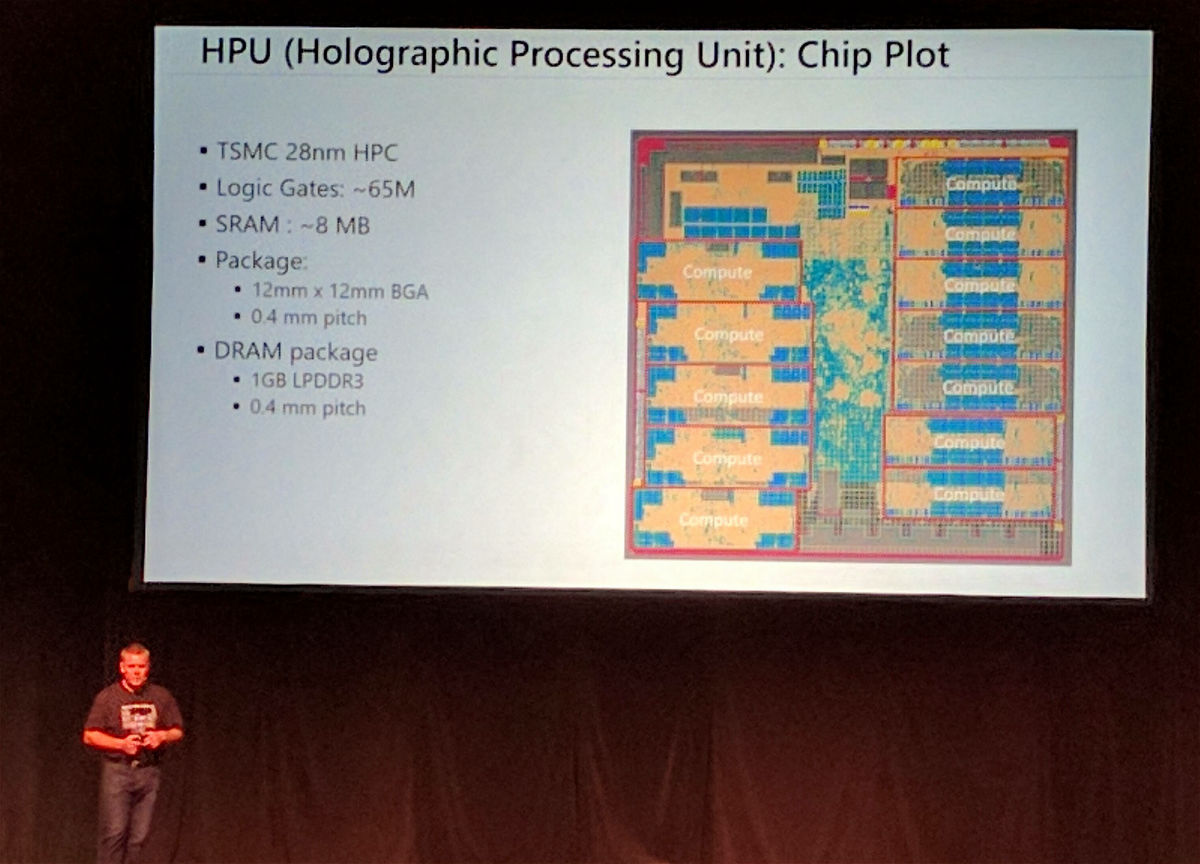
HPU collects data from various sensors installed in HoloLens and handles the action by user's gesture. Each of the 24 DSP cores is designed to handle different tasks, and it seems that processing can be done faster than running the same code with a general CPU.
The HPU has a 1 GB memory with a 14 nmAtom x86 Cherry Trail, This SoC plays the role of launching Windows 10 and applications on HoloLens display and enhances immersion when using it.

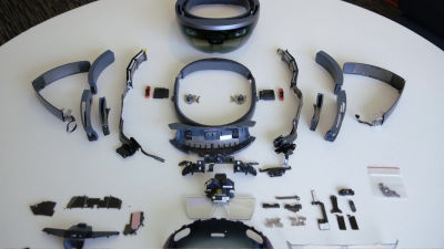
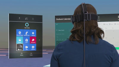
HoloLens, as if it had jumped out of the movie world, enabling mixed reality (MR) with real world and virtual world (VR) mixed in, in April 2016Developer version appearsAnd on August 18thCorporate kit releasedIt was done. It is unknown at the time of article creation when the commercial version for the general public will be released.
Related Posts:


in Hardware, Posted by darkhorse_log